Scanning electron microscope

Active Publication Date: 2005-07-07
HITACHI HIGH-TECH CORP
View PDF23 Cites 13 Cited by
  • Summary
  • Abstract
  • Description
  • Claims
  • Application Information

AI Technical Summary

Benefits of technology

[0018] The electron beam microscope of the present invention creates a histogram of a sample image, and can find a minimum frame count from a calculated probe current amount based on halftone levels near the border of a sample and a background. By observing the sample under the conditions of the calcu

Problems solved by technology

However, the results of recent investigations have revealed that the ArF resist is highly vulnerable to electron beam irradiation, and when a formed pattern is observed or measured with a scanning electron microscope, the scanning of a converged electron beam causes a condensation reaction in a base acrylic resin or the like, resulting in a reduction in volume (hereinafter called “slimming”) and an eventual change in the shape of a circuit pattern.
However, a reduction in the irradiation density of an electron bea

Method used


Image

  • Scanning electron microscope
  • Scanning electron microscope
  • Scanning electron microscope

Examples


Embodiment Construction

[0029] In the following, embodiments of the present invention will be described with reference to the accompanying drawings.

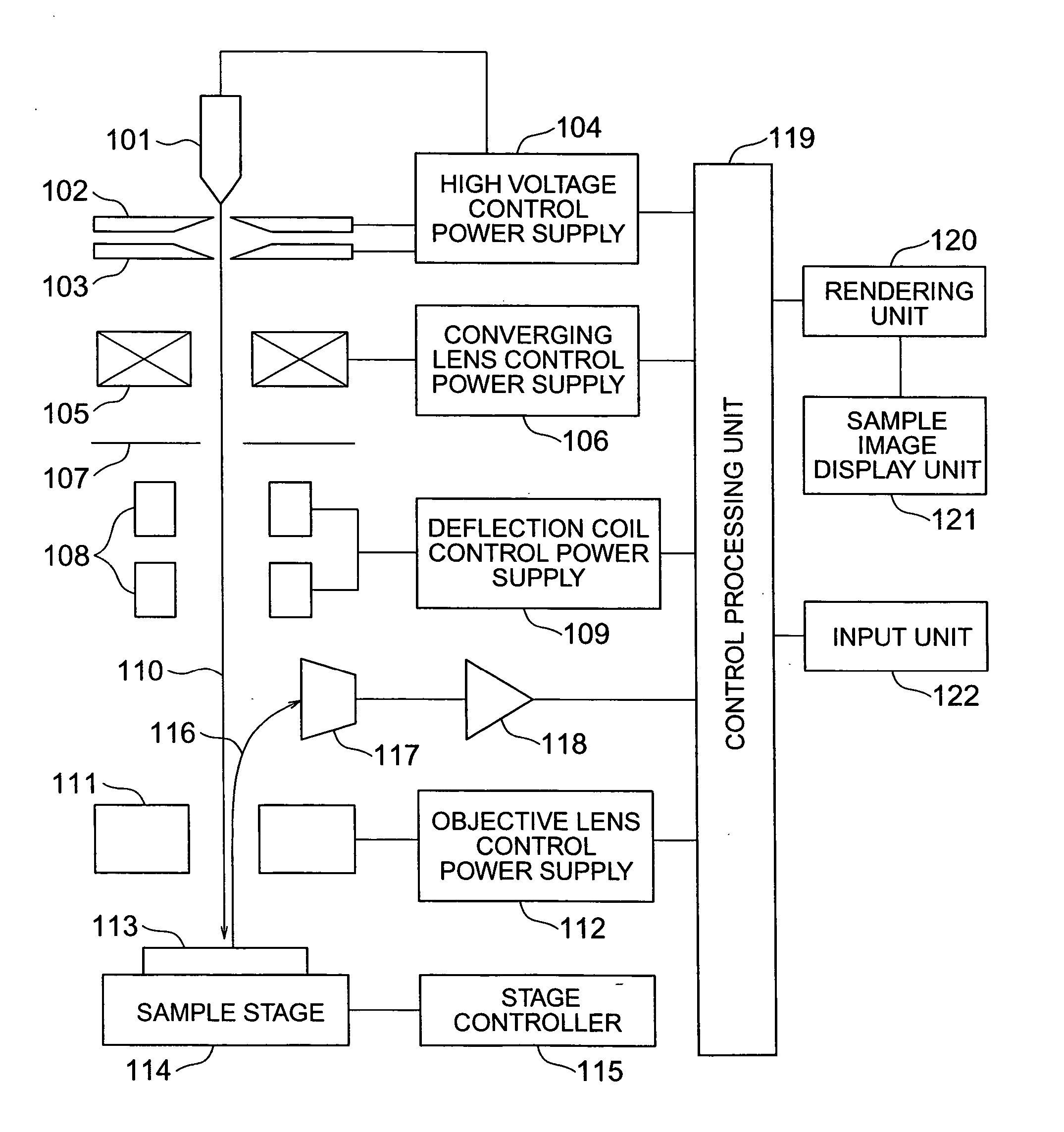
[0030]FIG. 1 is a block diagram generally illustrating a scanning electron microscope according to the present invention. A voltage is applied between a cathode 101 and a first anode 102 by a high voltage control power supply 104 which is controlled by a control processing unit 119 to draw a predetermined emission current from the cathode 101. Since an accelerating voltage is applied between the cathode 101 and a second anode 103 by the high voltage control power supply 104 controlled by the control processing unit 119, a primary electron beam 110 emitted from the cathode 101 is accelerated to travel to a subsequent lens system. The primary electron beam 110 is converged by a convergence lens 105 controlled by a convergence lens control power supply 106, and an unnecessary region of the primary electron beam 110 is removed by an aperture plate 107. Then, the p...


PUM


Abstract

In a scanning electron microscope, slimming is reduced by reducing a frame count. As the frame count is reduced, the amount of detected secondary electrons decreases, so that a probe current amount is increased to emit an increased amount of detected secondary electrons. A primary electron beam is scanned on a sample, a histogram is created, and the histogram is second-order differentiated to calculate a level of halftone at which a sample image changes in contrast, and to calculate the probe current amount. By adjusting the frame count suitable for the calculated probe current amount, and the contrast suitable for the sample image, the slimming of the sample is limited, and a highly visible sample image is generated for length measurement.

Description

BACKGROUND OF THE INVENTION [0001] The present invention relates to a scanning electron microscope for observing a miniature pattern to measure dimensions thereof, and more particularly, to a scanning electron microscope for observing and measuring a sample, the shape of which can be deformed by an electron beam irradiated thereto. [0002] Scanning electron microscopes (SEM) are widely used in manufacturing and testing steps of a functional product such as a semiconductor device, a thin film magnetic head, and the like, which are fabricated by micro-machining the surface thereof, for measuring widths of processed patterns and inspecting the appearance of resulting products. The scanning electron microscope is an apparatus for forming the image of a sample by narrowing down an electron beam emitted from an electron source with a converging lens or an objective lens which makes use of an interaction of a magnetic field or an electric field with the electron beam, one-dimensionally or t...

Claims


Application Information

Patent Timeline
IPC IPC(8): G01N23/225G21K7/00H01J37/22H01J37/28
CPCG01N23/225H01J2237/22H01J37/28
Inventor FUJITA, MASASHIKAWADA, HIROKIIWAMA, SATORU
Owner HITACHI HIGH-TECH CORP
Why Eureka
Try Eureka