High performance nitride-based light-emitting diodes

a light-emitting diode, high-performance technology, applied in the direction of basic electric elements, electrical apparatus, semiconductor devices, etc., can solve the problems of reducing the external quantum efficiency of conventional light-emitting diodes to less than 20%, reducing the external quantum efficiency of conventional light-emitting diodes, and reducing the defect of the nitride semiconductor epitaxy layer. defects, the effect of improving the internal quantum efficiency of the diod

Inactive Publication Date: 2005-07-07
FORMOSA EPITAXY INCORPORATION
View PDF6 Cites 63 Cited by
  • Summary
  • Abstract
  • Description
  • Claims
  • Application Information

AI Technical Summary

Benefits of technology

[0010] In addition, by matching the refraction index of the light extraction layer and the refraction index of the substrate, the present invention greatly improves the external quantum efficiency of the diode.
[0011] Furthermore, the present invention uses the light extraction layer to greatly reduce the defects of the nitride semiconductor epitaxy layer, and improves the internal quantum efficiency of the diode.
[0012] The present invention provides a simple structure for pre-epitaxy manufacturing process in order to improve the external quantum efficiency of the diode.
[0013] To solve the second part of the problems described in the aforementioned methods, the present invention uses the following method: first, growing a sacrificial layer in a pattern on the Al2O3 substrate, and then growing a nitride semiconductor epitaxy layer on top of the sacrificial layer. When the light-emitting structure of the nitride semiconductor and the substrate with high thermoconductivity are bound together by the binding layer, the sacrificial layer can be entirely etched away by a chemical solution used in a chemical etching process. Finally, the light-emitting structure of the nitride semiconductor is placed on the substrate with the high thermoconductivity. Because the substrate has high thermoconductivity, the diode can operate at high electrical current in order to improve the external quantum efficiency of the diode.
[0014] In addition, the use of a sacrificial layer in the present invention can reduce the defects of the nitride semiconductor epitaxy layer, and improves the internal quantum efficiency of the diode.
[0015] The present invention provides a simple structure for pre-epitaxy manufacturing process in order to manufacture a high power nitride-based light-emitting diode.

Problems solved by technology

The external quantum efficiency of conventional light-emitting diodes suffers from the failure of emitted light penetration, resulted from the refraction index difference between the semiconductor material and the external material.
Therefore, most of the emitted light runs and is absorbed inside the diode, and this results in reducing the external quantum efficiency to less than 20%.
However, the proposed method is difficult to materialize and has a poor yield rate.
However, in realistic application, the life span of this type of diodes is still unsatisfactorily short.
This also reduces the effective light-emitting area on the die.
Furthermore, because the substrate is made of material with low thermoconductivity, the diodes are not suitable for operating at high electrical current.
However, this method is difficult to materialize and also has a poor yield rate.
All the aforementioned methods suffer the drawbacks and limitations of the conventional nitride-based light-emitting diodes.

Method used


Image

  • High performance nitride-based light-emitting diodes
  • High performance nitride-based light-emitting diodes
  • High performance nitride-based light-emitting diodes

Examples


Embodiment Construction

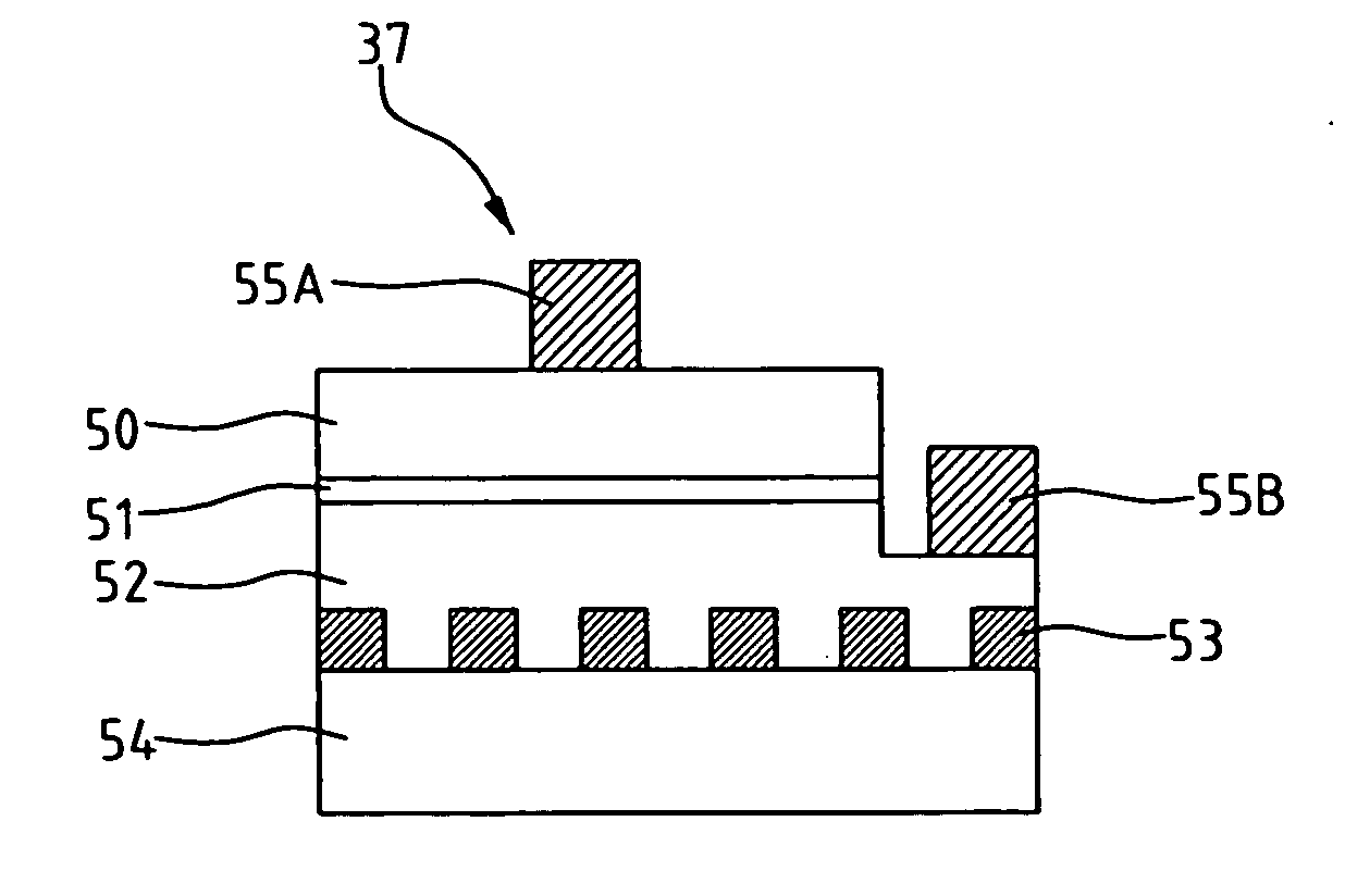
[0047] To achieve the objects described in the first part of the summary, the present invention grows a light extraction layer on the substrate before the epitaxy growth process. Then, a nitride semiconductor epitaxy layer is grown on the light extraction layer. After the micro-lithography, evaporation, etching, pressing, and dicing steps to fabricate the light-emitting diode. When the electrical current flows through the diode, the light reaches the light extraction layer and changes its traveling path before the light emitted from active layer reaching the substrate. Therefore, the light that would be absorbed previously by the epitaxy layer in the conventional techniques is able to penetrate the epitaxy layer and emits from the diode. Furthermore, by matching the refraction index of the light extraction layer and the refraction index of the substrate, it is able to greatly improve the external quantum efficiency.

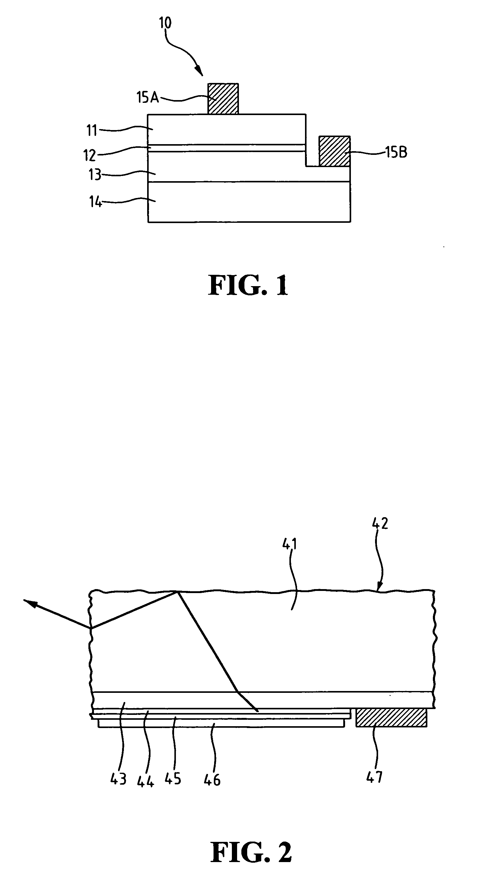
[0048] Referring to FIG. 1, a conventional nitride-based light-emit...


PUM


Abstract

A nitride-based light-emitting diode is provided, including a substrate having a light extraction layer grown on the substrate, and a nitride semiconductor epitaxy layer grown on the light extraction layer. The external quantum efficiency is improved by changing the traveling path of the emitted light and by matching the refraction index between the light extraction layer and the substrate. Also, a high power nitride-based light-emitting diode having a sacrificial layer is disclosed. A sacrificial layer is used for growing a light-emitting structure, and a binding layer made of two or more metals or alloys is used to bind the grown light-emitting structure and a substrate with high thermoconductivity. The sacrificial layer is later entirely etched away with a chemical solution used in a chemical etching process, and the nitrogen epitaxy structure is placed on the substrate with high thermoconductivity so that the diode can operate at high electrical current to improve external quantum efficiency.

Description

FIELD OF THE INVENTION [0001] The present invention relates to a nitride-based light-emitting diode and, more particularly, to a nitride-based light-emitting diode grown on a substrate with a light extraction layer. [0002] The present invention also relates to a high power nitride-based light-emitting diode and, more particularly, to a high power nitride-based light-emitting diode grown on a substrate with a sacrificial layer. BACKGROUND OF THE INVENTION [0003] The external quantum efficiency of conventional light-emitting diodes suffers from the failure of emitted light penetration, resulted from the refraction index difference between the semiconductor material and the external material. Take nitride-based light-emitting diode as example. The refraction index of the nitride semiconductor grown on the substrate is about 2.0-2.5, the refraction index of the Al2O3 substrate is 1.77, while the refraction index of epoxy resin used in conventional packaging methods is 1.5. Therefore, mo...

Claims


Application Information

Patent Timeline
Patent Type & Authority Applications(United States)
IPC IPC(8): H01L33/32
CPCH01L33/32H01L33/22
Inventor FANG, CHAO-YIYANG, KUANG-NENGCHIEN, FEN-RENCHEN, LUNG-CHIEN
Owner FORMOSA EPITAXY INCORPORATION
Why Eureka
Try Eureka