Use of gold surface finish on a copper wire-bond substrate, method of making same, and method of testing same

a technology of copper wire bonding and surface finish, which is applied in the direction of resistive material coating, printed circuit assembling, metallic pattern materials, etc., can solve the problems of significant corrosion, unacceptable yield loss during assembly process, and corrosion of residual bus bars

Inactive Publication Date: 2005-07-07
INTEL CORP
View PDF5 Cites 15 Cited by
  • Summary
  • Abstract
  • Description
  • Claims
  • Application Information

AI Technical Summary

Problems solved by technology

At the edge of the array where a bus bar is exposed, this process flow often causes significant corrosion particularly if it is copper.
The result is an unacceptable yield loss during assembly process, including wire-bonding process and singulation process or a field failure after the article has been placed into service.
During and after the wire bonding process, corrosion can occur in the exposed residual of the bus bar.
Other corrosion can occur where the wire bond meets the bond finger.
Once corrosion begins, a variable and unpredictable contact resistance (CRES) occurs between the wire bond and the bond finger.
Additionally during e-test, a copper scumming of the probe tip requires frequent and unscheduled cleaning.

Method used


Image

  • Use of gold surface finish on a copper wire-bond substrate, method of making same, and method of testing same
  • Use of gold surface finish on a copper wire-bond substrate, method of making same, and method of testing same
  • Use of gold surface finish on a copper wire-bond substrate, method of making same, and method of testing same

Examples


Embodiment Construction

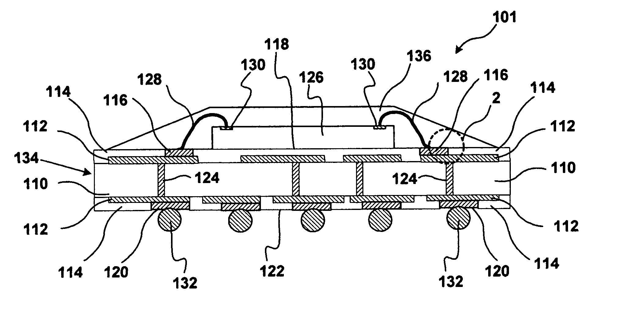
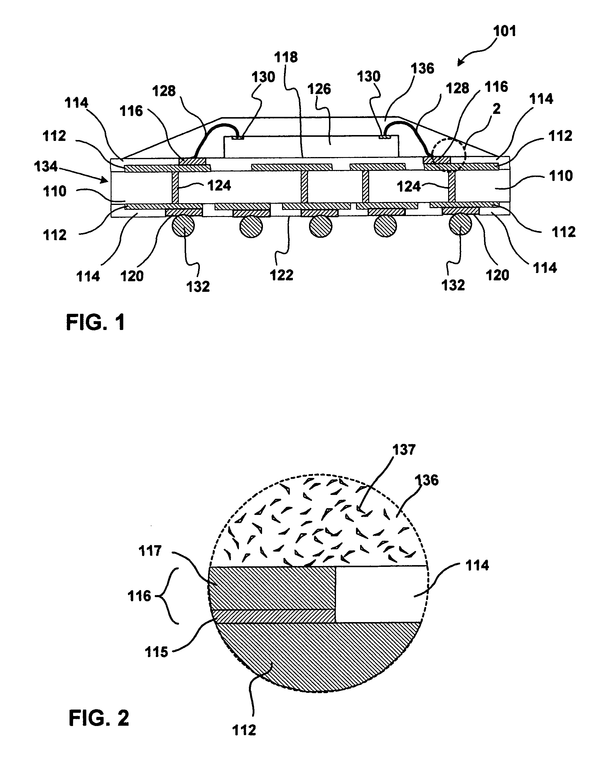
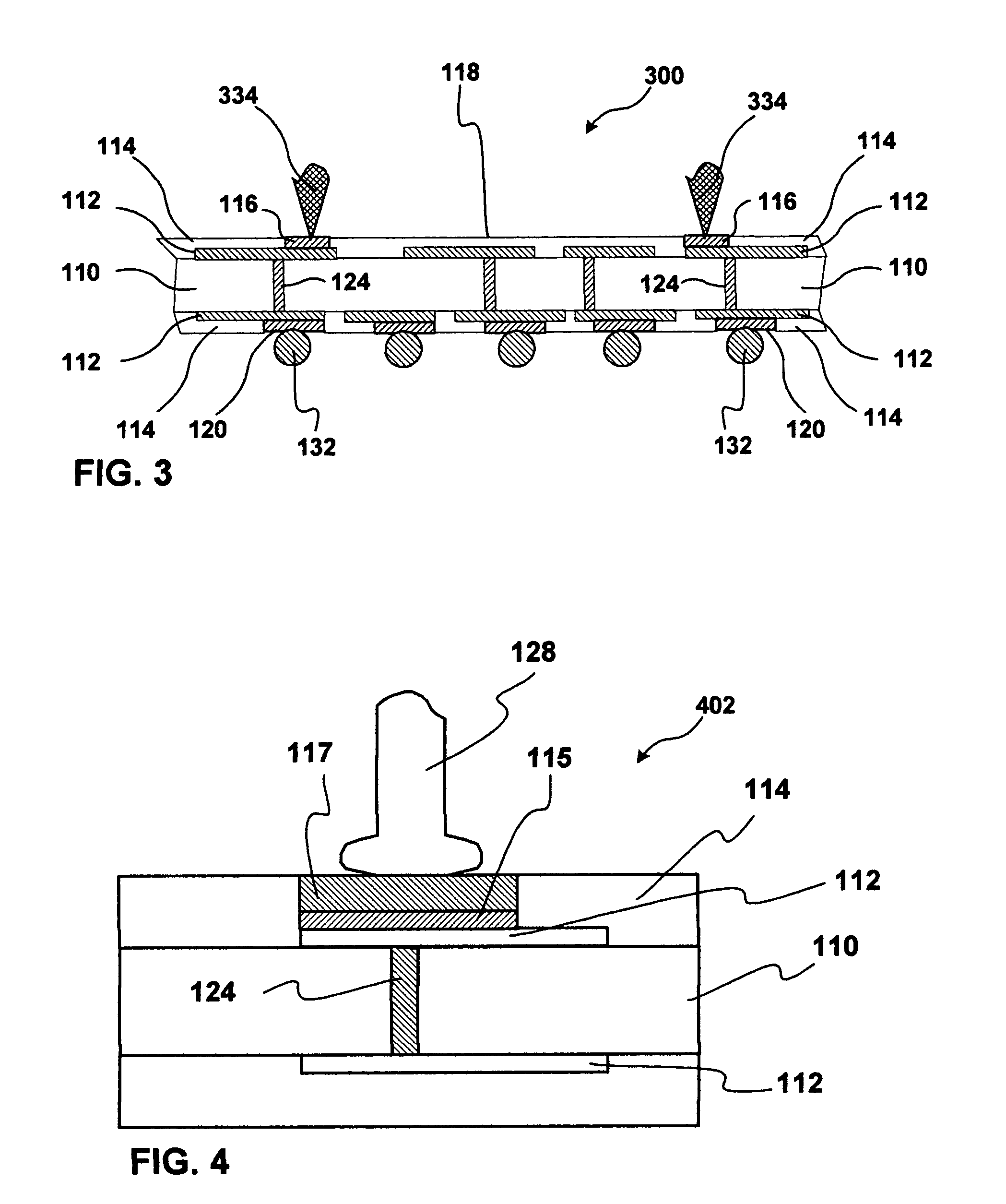
[0012] The following description includes terms, such as upper, lower, first, second, etc. that are used for descriptive purposes only and are not to be construed as limiting. The embodiments of a device or article described herein can be manufactured, used, or shipped in a number of positions and orientations. The terms “die” and “processor” generally refer to the physical object that is the basic workpiece that is transformed by various process operations into the desired integrated circuit device. A board is typically a copper-overlay structure that is insulated and that acts as a mounting substrate for the die. A die is usually singulated from a wafer, and wafers may be made of semiconducting, non-semiconducting, or combinations of semiconducting and non-semiconducting materials.

[0013] Reference will now be made to the drawings wherein like structures will be provided with like reference designations. In order to show the structure and process embodiments most clearly, the draw...


PUM

PropertyMeasurementUnit
thicknessaaaaaaaaaa
thicknessaaaaaaaaaa
thicknessaaaaaaaaaa

Abstract

A wire-bonding substrate is described. The wire-bonding substrate includes a copper metallization and a gold surface finish disposed above and on the copper metallization. The gold surface finish completes a structure that includes at least one of a bond finger for wire bonding of a first side of the substrate, and a land pad for a ball attach on a second side of the substrate. A process of forming the surface finish is also disclosed. An electronic package is also disclosed that uses the surface finish on the wire-bonding substrate. A method of assembling an electronic package is also disclosed that includes the surface finish on the wire-bonding substrate. A computing system is also described that includes the surface finish on the wire-bonding substrate.

Description

TECHNICAL FIELD [0001] Disclosed embodiments relate to wire bonding for a metallization process flow. More particularly, disclosed embodiments relate to an electroless plating process flow that can be followed by in situ electrical testing (e-test), and for a wire-bonding process flow upon a copper bond finger or a copper land for a ball attach. BACKGROUND INFORMATION [0002] Electroplating metallization process flows are carried out to prepare bond fingers and land pads for electrical connections upon substrates. Such substrates include very-fine ball-grid array (vfBGA), stacked chip-scale package (SCSP), plastic ball-grid array (PBGA) and others. During the wire bonding process, a bond wire is used to make contact between a board layout and a metallization pad on a chip. At the edge of the array where a bus bar is exposed, this process flow often causes significant corrosion particularly if it is copper. The result is an unacceptable yield loss during assembly process, including wi...

Claims


Application Information

Patent Timeline
Patent Type & Authority Applications(United States)
IPC IPC(8): C23C28/02C23C30/00H01L23/498H05K3/24H05K3/34
CPCC23C30/00H01L2224/45124H01L23/49866H01L24/45H01L2224/45144H01L2224/48091H01L2924/01012H01L2924/0102H01L2924/01038H01L2924/01046H01L2924/01077H01L2924/01078H01L2924/01079H01L2924/14H01L2924/1433H01L2924/15311H05K3/244H05K3/3457H05K2203/049H05K2203/1572H01L23/49811H01L2224/45139Y10T428/24917H01L2924/01047H01L24/48H01L2924/01019H01L2924/01087H01L2924/01013H01L2924/01028H01L2224/45169H01L2224/45644H01L2224/48227H01L2924/01015H01L2924/00014H01L2924/00H01L2924/181H01L2924/00012H01L2224/45015H01L2924/207
Inventor TAGGERT, BRIANHACKITT, DALEMISRA, DILIP K.
Owner INTEL CORP
Why Eureka
Try Eureka