On-chip structure for electrostatic discharge (ESD) protection

a technology of electrostatic discharge and on-chip structure, which is applied in the direction of semiconductor devices, semiconductor/solid-state device details, electrical apparatus, etc., can solve the problems of huge current, ic's vulnerability to electrostatic discharge (esd), and the tendency to miniaturize the integrated circuit (ic) and other critical reliability problems, so as to achieve a wide range of effects, efficient and reliabl

Inactive Publication Date: 2005-07-14
INTERSIL INC
View PDF5 Cites 113 Cited by
  • Summary
  • Abstract
  • Description
  • Claims
  • Application Information

AI Technical Summary

Benefits of technology

[0018] The presently disclosed SCR-based structure has been designed, fabricated, and measured with consistent design criteria to enable a tunable holding voltage for robust and versatile ESD protection. The structure has been designed, fabricated and measured in two complementary versions, n-type and p-type, each of them with slightly different characteristics. The SCR-based structure wil

Problems solved by technology

Microchips' size reduction has been traditionally the most important challenge in the semiconductor industry; however, reliability issues and robustness of the circuits present a bottleneck in the integrated circuit (IC) miniaturization tendency.
The IC's vulnerability to electrostatic discharge (ESD) is one of the most critical reliability problems.
The process results in a huge current, and when a microchip is subjected to ESD, the microchip is likely to be damaged.
At times, numerous ICs have been migrated to state-of-the-art CMOS technologies, but direct scaling can reduce the level of ESD protection accordingly.
As a result, IC's production tape outs are being considerably delayed mainly because products do not meet the ESD protection requirements.
Furthermore, even increasing the size of the traditional protection structures to levels comparable with the core circuit dimensions

Method used


Image

  • On-chip structure for electrostatic discharge (ESD) protection
  • On-chip structure for electrostatic discharge (ESD) protection
  • On-chip structure for electrostatic discharge (ESD) protection

Examples


Embodiment Construction

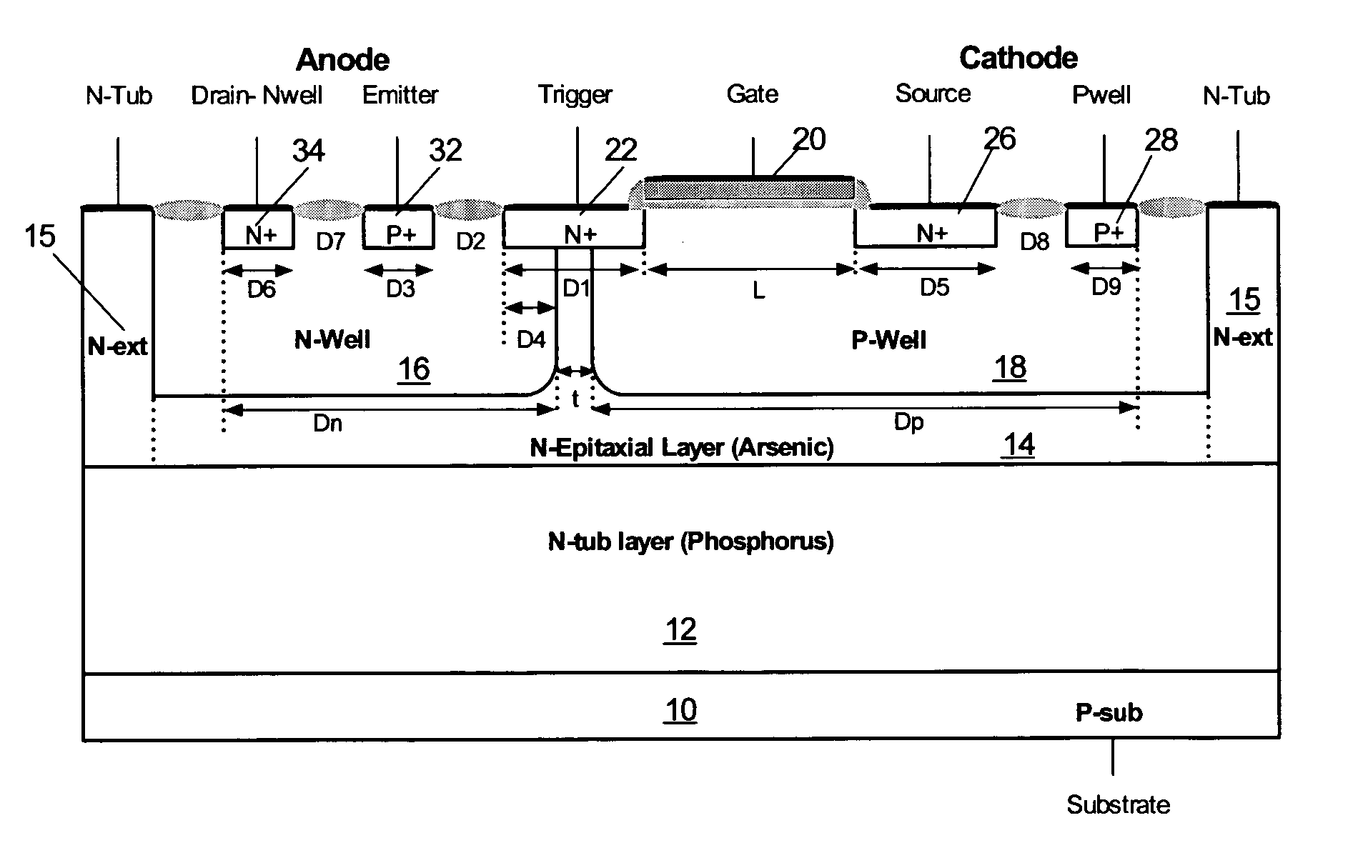
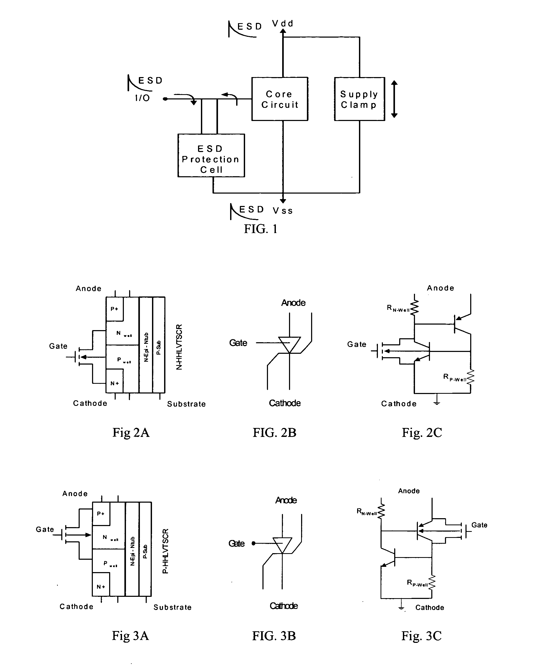
[0039] This disclosure presents an ESD protection solution by using the schematic presented in FIG. 1, and highly efficient silicon controlled rectifier (SCR) design, called the high holding voltage / low voltage trigger SCR (HHLVTSCR), for the supply clamp and I / O ESD protection cell shown in FIG. 1. The N-HHLVTSCR and P-HHLVTSCR possess a very low leakage current and a tunable holding voltage from less than 2 V to over 11 V.

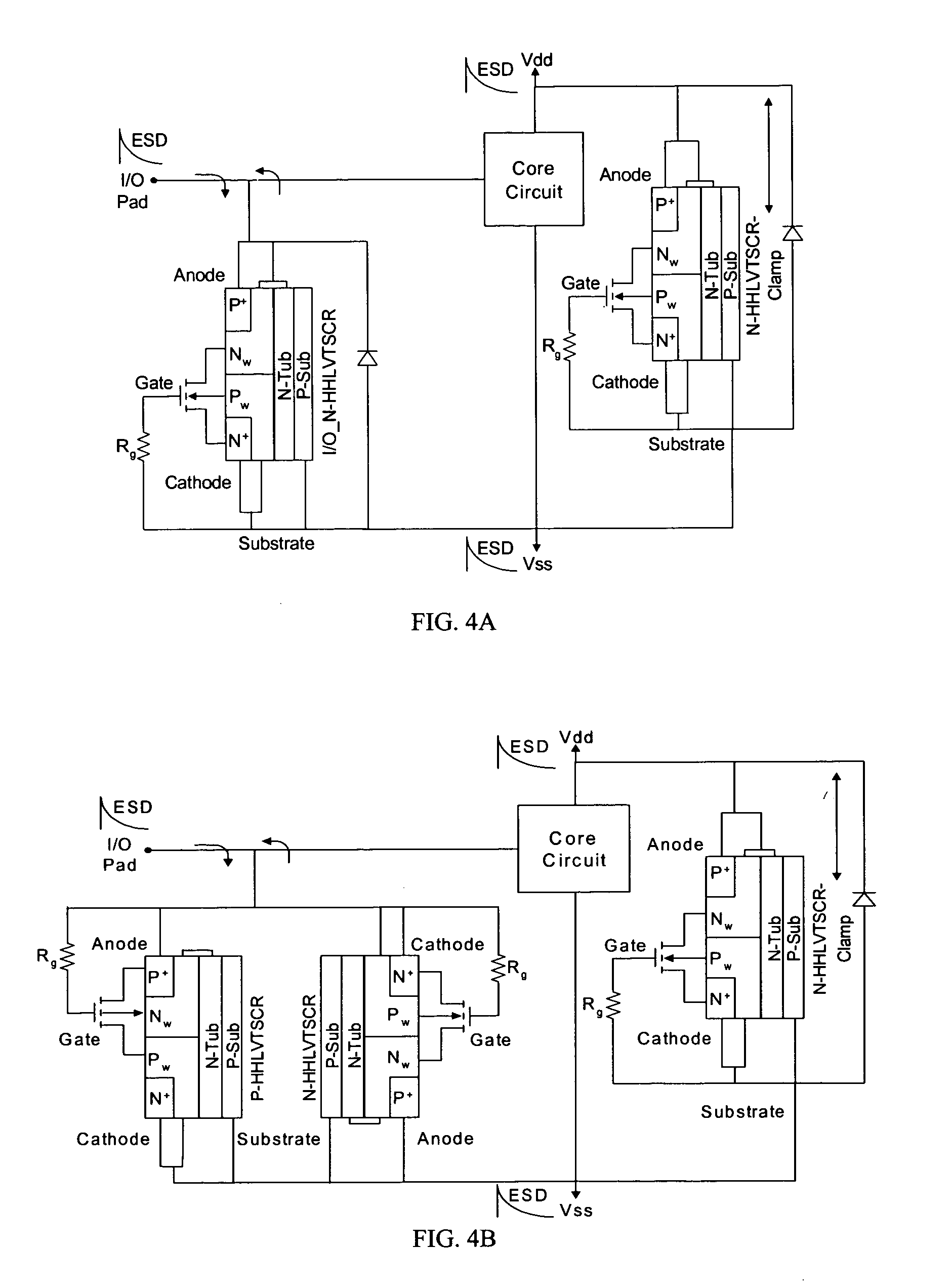
[0040] The schematic in FIG. 1 is slightly different from the schemes traditionally used for ESD protection. In our design, the complete ESD protection is accomplished with a bidirectional ESD protection, with only a ground reference at the I / O pads, and a bidirectional supply clamp. Based on this approach, either identical or different structures can be designed for the supply clamp and I / O protection cell, depending on the bias conditions during normal operation of the internal circuit. For instance, the signal swing at the I / O pad can be either within the ran...


PUM


Abstract

A complementary SCR-based structure enables a tunable holding voltage for robust and versatile ESD protection. The structure are n-channel high-holding-voltage low-voltage-trigger silicon controller rectifier (N-HHLVTSCR) device and p-channel high-holding-voltage low-voltage-trigger silicon controller rectifier (P-HHLVTSCR) device. The regions of the N-HHLVTSCR and P-HHLVTSCR devices are formed during normal processing steps in a CMOS or BICMOS process. The spacing and dimensions of the doped regions of N-HHLVTSCR and P-HHLVTSCR devices are used to produce the desired characteristics. The tunable HHLVTSCRs makes possible the use of this protection circuit in a broad range of ESD applications including protecting integrated circuits where the I/O signal swing can be either within the range of the bias of the internal circuit or below/above the range of the bias of the internal circuit.

Description

CROSS REFERENCE [0001] This application claims the benefit of and incorporates herein by reference provisional application Ser. No. 60 / 535,816, filed Jan. 13, 2003.FIELD OF THE INVENTION [0002] The present disclosure relates in general to electrostatic discharge protection in electronic circuits, and in particular to tunable high holding voltage silicon controlled rectifiers for latch-up free on-chip electrostatic discharge protection and the method of designing these devices. BACKGROUND OF THE INVENTION [0003] Microchips' size reduction has been traditionally the most important challenge in the semiconductor industry; however, reliability issues and robustness of the circuits present a bottleneck in the integrated circuit (IC) miniaturization tendency. The IC's vulnerability to electrostatic discharge (ESD) is one of the most critical reliability problems. ESD is an event that transfers a finite amount of charge from one object (i.e., human body, transmission lines, or metallic pie...

Claims


Application Information

Patent Timeline
IPC IPC(8): H01L27/02H01L29/72
CPCH01L29/7436H01L27/0262
Inventor SALCEDO, JAVIER A.LIOU, JUIN J.BERNIER, JOSEPH C.WHITNEY, DONALD K. JR.
Owner INTERSIL INC
Why Eureka
Try Eureka