
Method to reduce a capacitor depletion phenomena

a capacitor and depletion phenomenon technology, applied in the field of semiconductor devices, can solve the problems of deleterious depletion phenomena affecting the performance of capacitor cells, and achieve the effect of less risk of capacitor depletion phenomena

Inactive Publication Date: 2005-07-14
TAIWAN SEMICON MFG CO LTD
View PDF3 Cites 10 Cited by
  • Summary
  • Abstract
  • Description
  • Claims
  • Application Information

AI Technical Summary

Benefits of technology

[0007] It is another object of this invention to form a capacitor region with less risk of a capacitor depletion phenomena via implantation of the capacitor region in tapered silicon sidewall, exposed in a recessed portion of a shallow trench isolation (STI) structure.
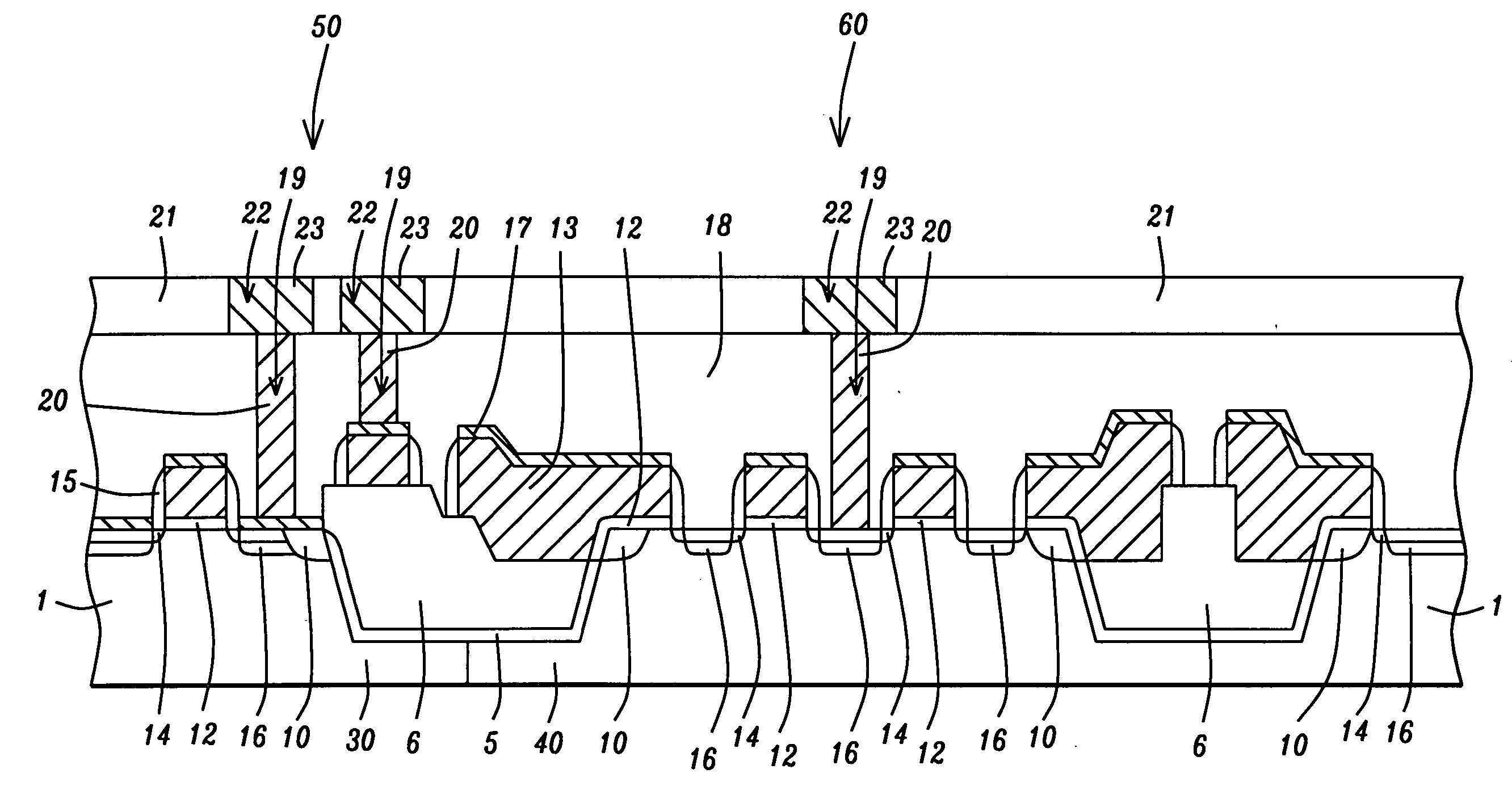
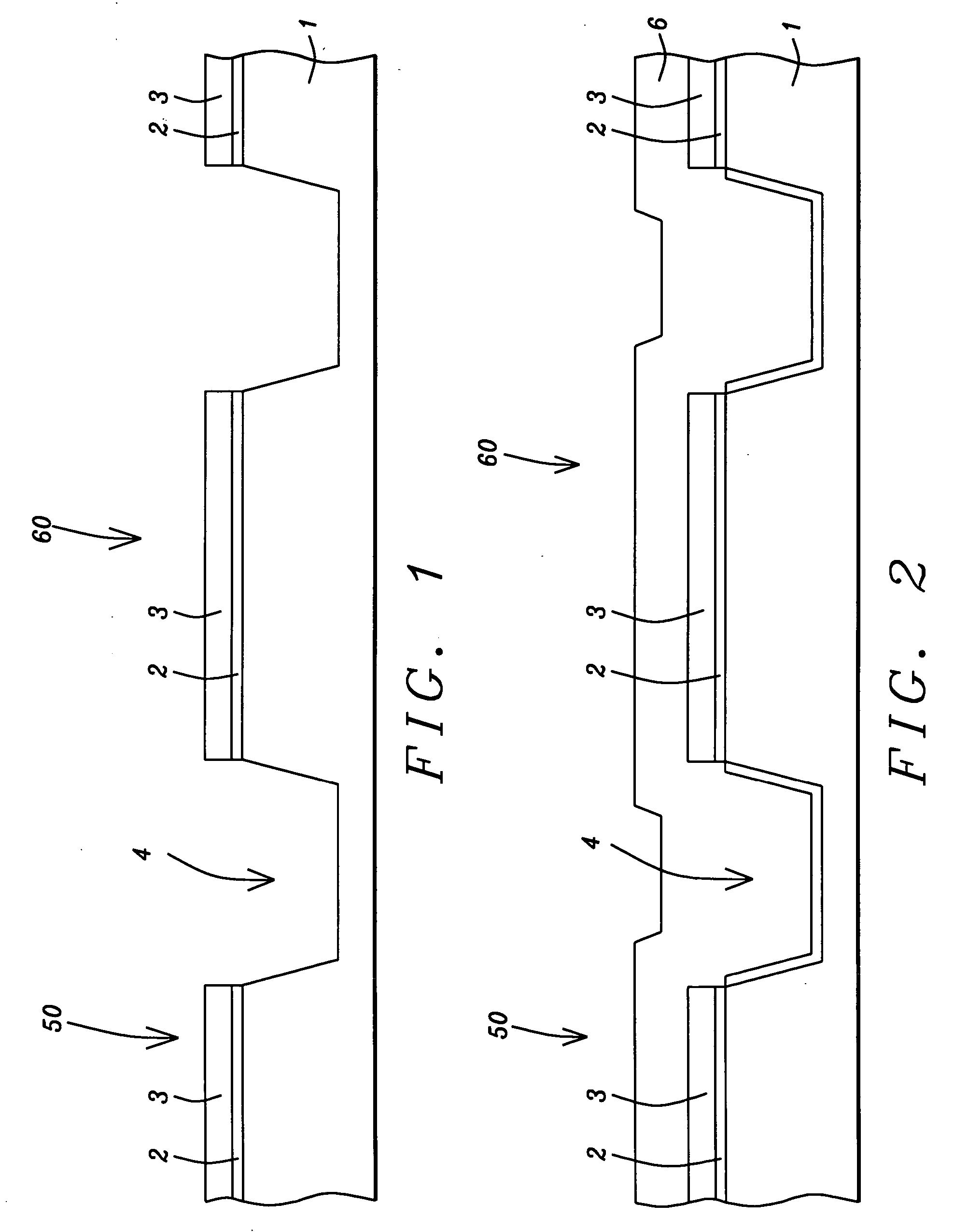
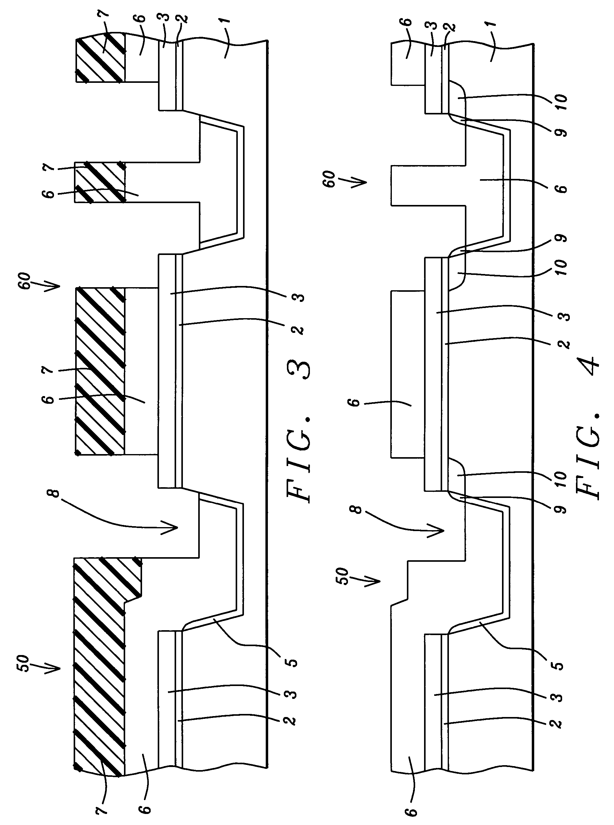
[0009] In accordance with the present invention a method of integrating the fabrication of a capacitor cell in a logic device process sequence featuring increased capacitor area and reduced risk of a capacitor depletion phenomena, via implantation of a capacitor region into a tapered silicon side wall exposed in an STI structure, will now be described in detail. After definition of shallow trench shapes in an insulator hard mask layer, as well as in top portions of a semiconductor substrate wherein the shallow trench shapes feature tapered side walls, an insulator liner layer is formed on all exposed surfaces of the shallow trench shapes. Deposition of another insulator layer results in insulator filled, shallow trench isolation (STI) structures. Photolithographic and dry etching procedures define an capacitor area in a portion of the semiconductor substrate to be used to accommodate a capacitor cell, accomplished via recessing of a top portion of the insulator layer in the STI structures, as well removal of exposed portions of the liner layer resulting in exposure of tapered silicon side walls. A capacitor region is next formed via implantation of specific ions into the tapered silicon side walls, and into a semiconductor region located underlying the insulator hard mask layer, adjacent to the recessed portion of the STI structure. After removal of the insulator hard mask layer a capacitor dielectric layer is formed on the surfaces of the capacitor region, the exposed tapered silicon side walls in the recessed portion of the STI structure, and a top portion of semiconductor region located adjacent to the recessed portion of the STI structure. The same capacitor dielectric layer is formed as a gate insulator layer in a logic device region. A conductive layer is deposited and patterned to define a capacitor plate structure as well as transfer gate structures in the capacitor cell region, and to define gate structures in the logic device region. Lightly doped source / drain (LDD) regions, insulator side wall spacers, and heavily doped source / drain regions are then formed in logic device region as well as in the capacitor cell region, allowing the path for the capacitance to be accessed.

Problems solved by technology

If specific photolithographic masking steps directed at exposing areas wherein capacitor regions will be formed via ion implantation procedures are marginalized, inadequate formation of the capacitor region will occur resulting in a capacitor depletion phenomena deleteriously influencing capacitor cell performance.

Method used


Image

  • Method to reduce a capacitor depletion phenomena
  • Method to reduce a capacitor depletion phenomena
  • Method to reduce a capacitor depletion phenomena

Examples


Embodiment Construction

[0012] The method of integrating the fabrication of a capacitor cell in a logic process sequence wherein increased capacitor area and reduced risk of a capacitor depletion phenomena are realized via implantation of a capacitor region into a tapered silicon side wall exposed in an STI structure, will now be described in detail. Semiconductor substrate 1, comprised of P type single crystalline silicon, featuring a crystallographic orientation, is used and schematically shown in FIG. 1. The fabrication of a capacitor cell will be shown in region 60 of semiconductor substrate 1, integrated with the fabrication of logic devices in region 50 of semiconductor substrate 1. Pad oxide layer 2, comprised of silicon oxide is formed at a thickness between about 50 to 300 Angstroms, on the surface of semiconductor substrate 1, via thermal oxidation procedures, or via low pressure chemical vapor deposition (LPCVD) or plasma enhanced chemical vapor deposition (LPCVD) procedures. Silicon nitride la...


PUM


Abstract

A method of integrating the fabrication of a capacitor cell and a logic device region, wherein the surface area of a capacitor region is increased, and the risk of a capacitor depletion phenomena is reduced, has been developed. After formation of insulator filled STI regions featuring tapered sides, a portion of the insulator layer in an STI region is recessed below the top surface of the semiconductor substrate exposing a bare, tapered side of the semiconductor substrate. Ion implantation into the tapered side of the portion of semiconductor substrate exposed in the recessed STI portion, as well as into a top portion of semiconductor substrate located adjacent to the recessed STI portion, results in formation of a capacitor region now greater in surface area than a counterpart capacitor region which is formed via implantation into only a top portion of semiconductor substrate. Growth of a gate insulator layer and definition of gate structures in the logic device region, also simultaneously forms a capacitor dielectric layer on the underlying capacitor region, as well as a capacitor plate structure in the capacitor cell region.

Description

BACKGROUND OF THE INVENTION [0001] (1) Field of the Invention [0002] The present invention relates to methods used to fabricate semiconductor devices, and more specifically to a method used to improve the integrity of a capacitor device. [0003] (2) Description of Prior Art [0004] The advent of micro-miniaturization, or the ability to fabricate semiconductor devices featuring sub-micron features, has allowed device fabrication costs to be reduced while also allowing the performance of these same devices to be increased. Advances in specific semiconductor fabrication disciplines such as photolithographic and dry etching has enabled smaller device features to be routinely obtained, thus allowing decreases in unwanted performance degrading capacitances to be realized. In addition integrated fabrication of specific elements such as capacitor structures, along with other semiconductor logic components have allowed process costs to be reduced. To minimize the number of cost consuming photo...

Claims


Application Information

Patent Timeline
Patent Type & Authority Applications(United States)
IPC IPC(8): H10B12/00
CPCH01L27/10894H01L27/1087H10B12/0387H10B12/09
Inventor CHIANG, MIN-HSIUNG
Owner TAIWAN SEMICON MFG CO LTD
Learn More