Shrunk low on-resistance DMOS structure

a dmos structure, low-resistance technology, applied in the direction of semiconductor devices, electrical apparatus, transistors, etc., can solve the problems of reducing the robustness of the device when operating at high current, the potential of the n+ source diffusion tends to differ from the potential of the p-, and the non-uniformity of the current density in the source region

Inactive Publication Date: 2005-07-14
STMICROELECTRONICS SRL
View PDF5 Cites 15 Cited by
  • Summary
  • Abstract
  • Description
  • Claims
  • Application Information

AI Technical Summary

Benefits of technology

[0022] By defining the implant window of the body connection plug diffusion dopant as an orthogonal strip of minimum linewidth, instead of a centered island area, the need of accounting for an adequate overlay is eliminated and overall renders the two masks that define (at their crossover) the implant area of the plug diffusion no longer critical.

Problems solved by technology

Problems arise from the fact that in operation, and especially at relatively high currents, the potential of the N+ source diffusion tends to differ from the potential of the P-body diffusion containing it.
Even a residual drawback of this approach causes current density non-uniformities in the source region because of charge carriers (electrons and holes) being collected through distinct contacts.
This reduces the robustness of the device when operating at high currents because of a premature turning on of the intrinsic parasitic bipolar junctions transistor (NPN or PNP).
This inevitably limits the possibility of reducing the width in the pitch direction of the elongated openings through the polysilicon gate layer.
These technological constraints relative to the definition of features within the poly openings of the source regions limit the possibility of further reducing the pitch of integration, and therefore, of the overall level of compactness that can be achieved with a certain manufacturing technology.
Also, the ability to reduce the on-resistance for unit area of integration of the structure is similarly limited.

Method used


Image

  • Shrunk low on-resistance DMOS structure
  • Shrunk low on-resistance DMOS structure
  • Shrunk low on-resistance DMOS structure

Examples


Embodiment Construction

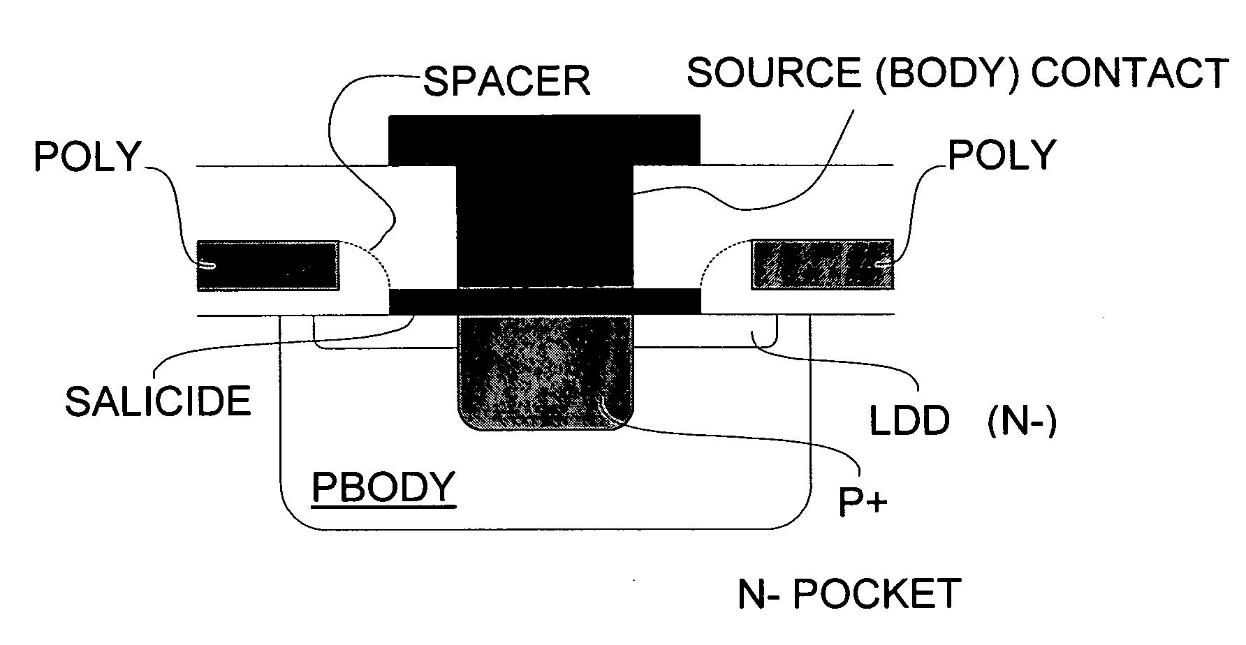
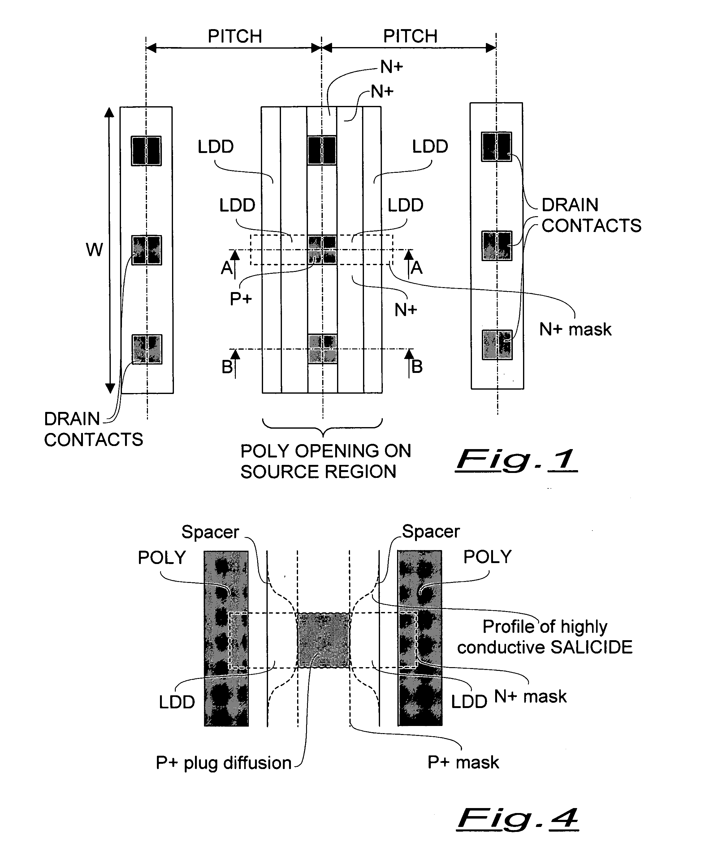
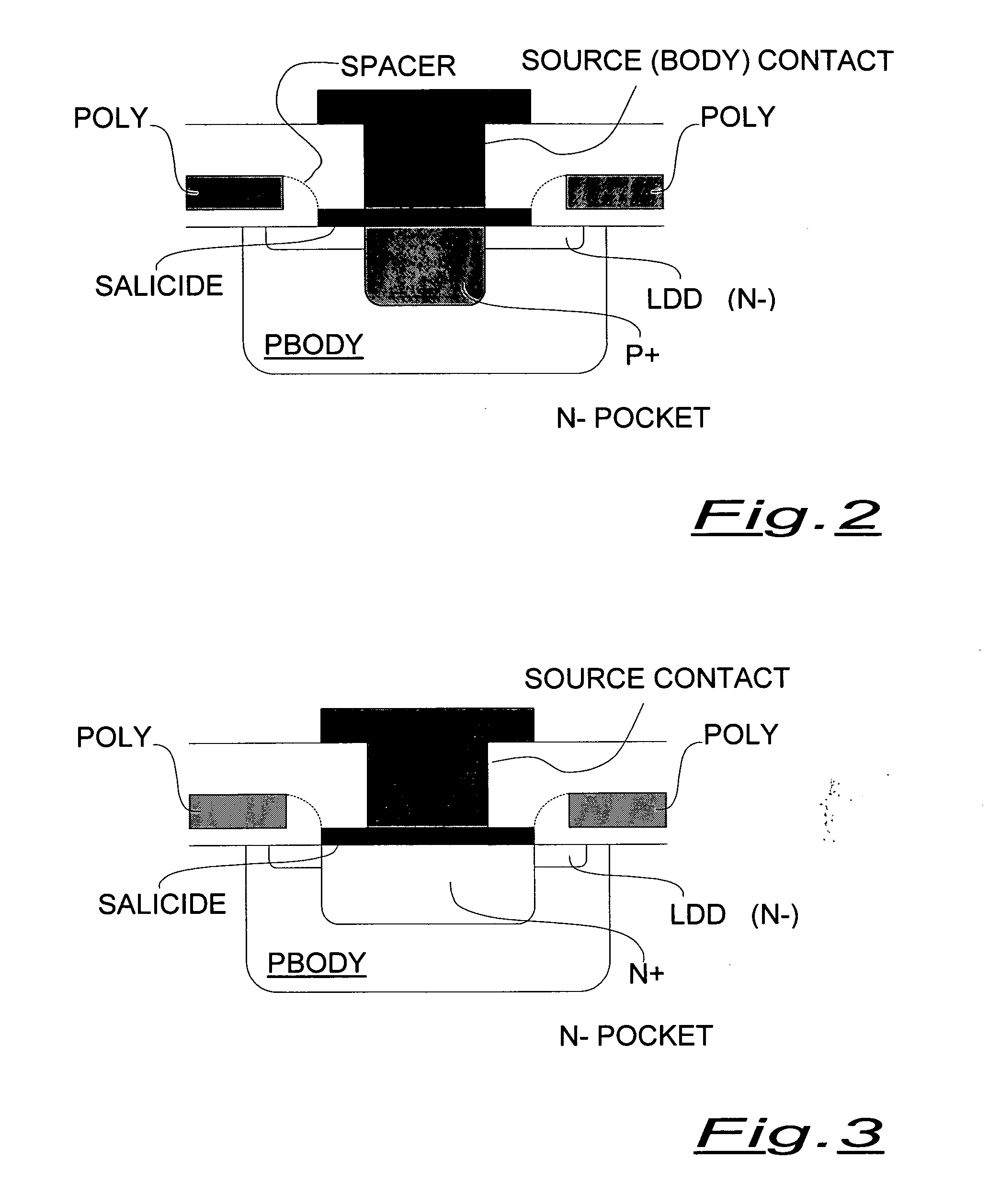
[0029] A basic layout view of an integrated LDMOS N-channel structure according to the present invention is shown in FIG. 1, while FIGS. 2 and 3 are partial cross-sectional views along the section planes A-A and B-B, respectively.

[0030] As may be clearly observed in the layout view of FIG. 1, the N+ mask used for implanting the source region in self-alignment with the spacers formed on the edges of definition of the opening through the polysilicon gate layer (POLY), masks from the N+ implant an orthogonal strip across the full width of the poly opening, practically leaving in the masked area only the LDD N− source diffusion. This represents a discontinuity of the N+ source diffusion in the source region defined by the opening through the polysilicon layer, along with the W direction of the integrated LDMOS structure.

[0031] According to a preferred embodiment, the N+ mask may be defined with the minimum linewidth of the process of fabrication, like the source contacts.

[0032] Anoth...


PUM


Abstract

The on resistance per unit area of integration of a DMOS structure is reduced beyond the technological limits of a mask that is defined based upon the continuity of a heavily doped superficial silicon region along the axis of the elongated source island openings through the polysilicon gate layer in the width direction of the integrated structure. The mask no longer needs to be defined with a width (in the pitch direction) sufficiently large to account for the overlay of two distinct and relatively critical masks. These two masks are the source implant mask and the body contacting plug diffusion implant contact opening mask. Such a constraint of the prior techniques restricting the opening through the polysilicon gate layer to safely ensure an appropriate distance of the body connection plug diffusion dopant profile from the definition edges of the polysilicon is overcome by defining the body connection plug diffusion implant area by way of a mutual orthogonality between two no longer critical masks that may both be defined at minimum linewidth of the fabrication process.

Description

FIELD OF THE INVENTION [0001] The present invention relates to integrated circuits, and in particular, to a compactly integrated DMOS structure with enhanced characteristics for withstanding high currents while retaining a low on-resistance. BACKGROUND OF THE INVENTION [0002] A DMOS structure includes a drain region, a source region and a gate defined over a channel region. In the case of an N-channel device, the source-body region is formed with respect to a purposely defined opening in a polysilicon gate layer, and includes a P-body diffusion formed inside an N-pocket. A single or, more commonly, a shallow N− and a deeper N+ source diffusion are formed in succession in the P-body region. This is done by successive implants self-aligned to the definition edges of the poly (gate) opening and to the dielectric spacers successively formed there along according to well known VLSI and ULSI fabrication techniques. A source contact is formed on the N+ source diffusion. Of course, the type...

Claims


Application Information

Patent Timeline
Patent Type & Authority Applications(United States)
IPC IPC(8): H01L21/336H01L29/06H01L29/08H01L29/417H01L29/45H01L29/78
CPCH01L29/0696H01L29/0847H01L29/41758H01L29/7801H01L29/456H01L29/66674H01L29/41775H01L29/1095H01L29/0869H01L29/66689H01L29/0865H01L29/665H01L29/086H01L29/7816
Inventor BRAMBILLA, DANIELE ALFREDO
Owner STMICROELECTRONICS SRL
Why Eureka
Try Eureka