Semiconductor device and cell

Active Publication Date: 2005-07-14
SOCIONEXT INC
View PDF4 Cites 1 Cited by
  • Summary
  • Abstract
  • Description
  • Claims
  • Application Information

AI Technical Summary

Benefits of technology

[0011] Therefore, an object of the present invention is to provide a semiconductor device, in which variations in the power supply voltage and the

Problems solved by technology

If the degree of circuit integration is increased without changing the power supply voltage, the power consumption of the circuit increases.
The lower the threshold voltage is, the more likely it is that a transistor may malfunction because of voltage fluctuations due to noise.
However, if the number of power supply lines or the width thereof is increased, the area of the region in which the power supply line or the ground line is formed increases, thereby increasi

Method used


Image

  • Semiconductor device and cell
  • Semiconductor device and cell
  • Semiconductor device and cell

Examples


first embodiment

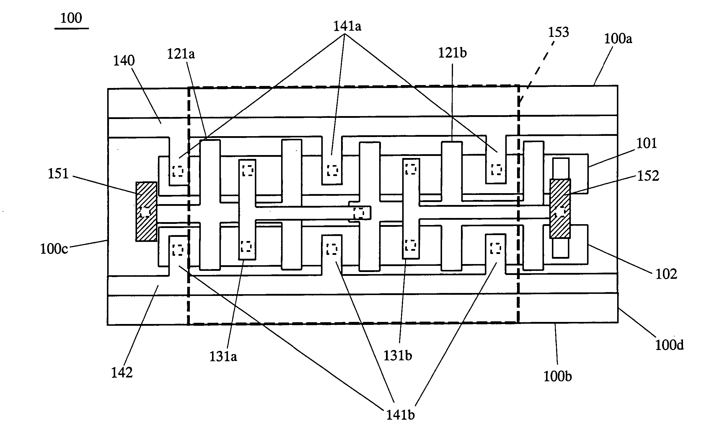
[0039]FIG. 1 is a layout diagram showing a cell 100 according to the first embodiment of the present invention. Referring to FIG. 1, the cell 100 includes a semiconductor substrate on which a P-channel transistor region 101 and an N-channel transistor region 102 are provided. On the semiconductor substrate, the cell 100 includes a preceding gate electrode section 121a (input gate), a subsequent gate electrode section 121b, a preceding drain electrode section 131a, a subsequent drain electrode section 131b (output drain), source electrodes 141a and 141b, a strap power supply line 140, a strap ground line 142, an input terminal 151 and an output terminal 152. The cell 100 has a rectangular shape whose perimeter is defined by long sides 100a and 100b and short sides 100c and 100d.

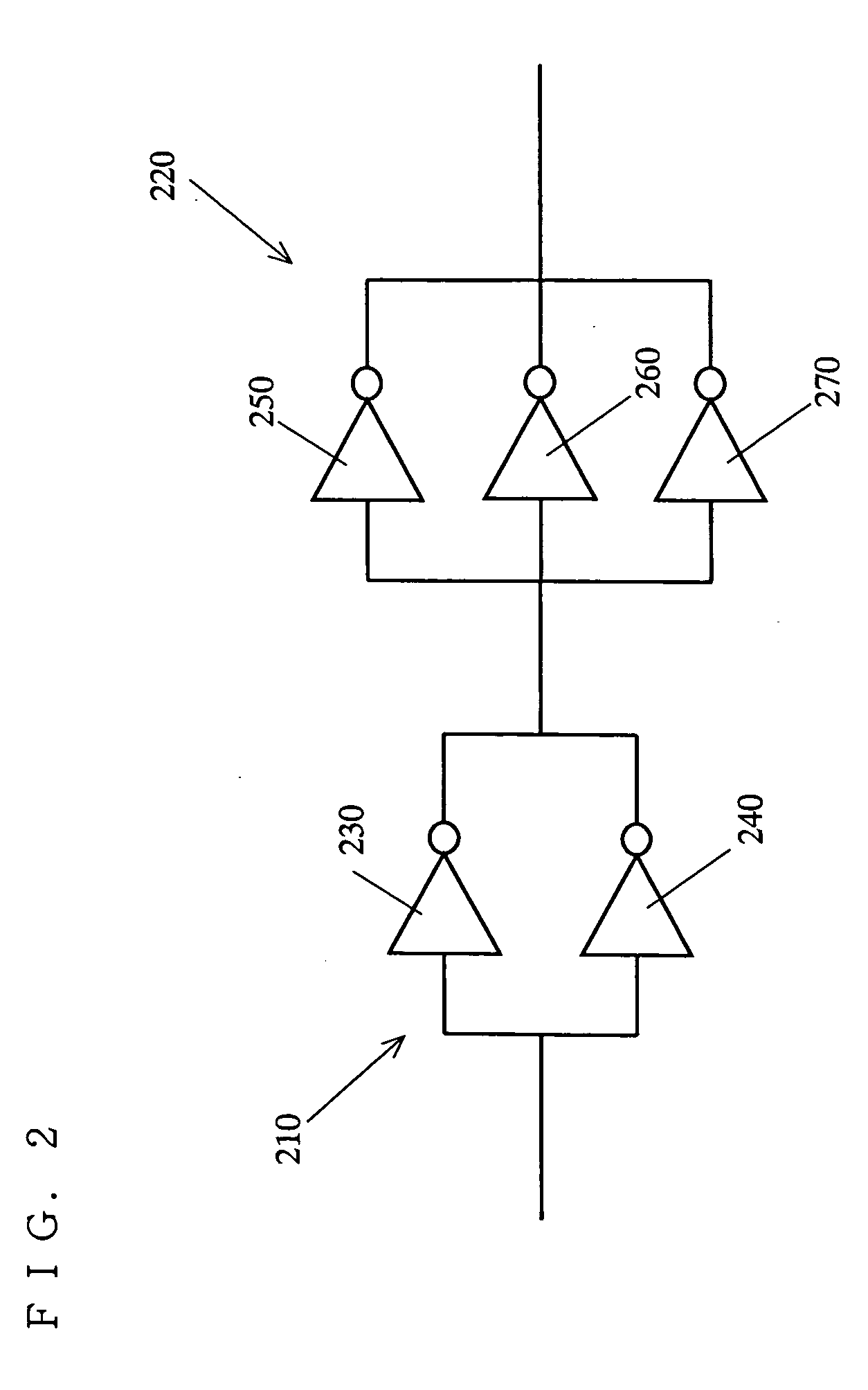
[0040] Referring to FIG. 2, the cell 100 is a logic circuit including a preceding block 210 and a subsequent block 220 connected in series with each other. The preceding block 210 includes two inverters 230 a...

second embodiment

[0061]FIG. 8 is a partially cutaway plan view showing a semiconductor device 800 according to the second embodiment of the present invention. FIG. 8 shows, on an enlarged scale, a portion of the cell arrangement region 310 of the semiconductor device 300 of the first embodiment shown in FIG. 3, for example. The semiconductor device 800 includes a plurality of cells 801, 802, 803, 804 and 805, a power supply line 500 and a ground line 600.

[0062] As with the cell of the first embodiment, each of the cells 801 to 805 includes a plurality of wiring layers on the semiconductor substrate including transistors, etc., formed thereon. Formed in the wiring layers are electrodes of the transistors, the strap power supply lines 140 for connecting the power supply lines to the electrodes, the strap ground lines 142, input terminals, output terminals, etc. The strap power supply lines 140 and the strap ground lines 142 are provided in a layer lower than the layer in which power supply line passi...

third embodiment

[0067]FIG. 9A and FIG. 9B are partially cutaway plan views showing semiconductor devices 900 and 901, respectively, according to the third embodiment of the present invention. The semiconductor device 900 includes power supply line routable cells 931, 933, 936, 937, 938, 939 and 941 as described above in the first and second embodiments, cells 932, 934, 935 and 940 that do not have power supply line passing regions, the power supply line 500 and the ground line 600. The cells 931, 933, 936, 937, 938, 939 and 941 each have a multilayer wiring structure with a plurality of wiring layers provided on a semiconductor substrate, as described above in the first embodiment. Power supply line passing regions 931a, 933a, 933b, 936a, 937a, 938a, 939a and 941a are provided in the same wiring layer. The concept for the power supply line passing region is as described above in the first embodiment, and will not be further described in the present embodiment. In the semiconductor device 900 shown ...


PUM


Abstract

A cell 100 includes three wiring layers (a gate electrode layer, a source/drain electrode layer and a terminal layer) on a semiconductor substrate including transistors formed thereon. One of the wiring layers (the terminal layer) in which input terminals 151 and output terminals 152 for connecting the cell to another cell are formed includes a power supply line passing region 153 through which a power supply line for supplying a power supply voltage and a ground voltage from an external power supply to the transistors in the cell can be provided.

Description

BACKGROUND OF THE INVENTION [0001] 1. Field of the Invention [0002] The present invention relates to a semiconductor device and a cell. [0003] 2. Description of the Background Art [0004] Along with recent advancements in the miniaturization techniques, the degree of integration of integrated circuits (semiconductor devices) is increasing. FIG. 12 is a partially cutaway plan view showing a conventional semiconductor device 1200 as disclosed in Japanese Laid-Open Patent Publication No. 2002-261245. The semiconductor device 1200 includes a plurality of cells 1201, a power supply line 1203b, a ground line 1203a, a strap power supply line 1202b and a strap ground line 1202a. Each cell 1201, being a circuit component forming a circuit together with other cells, may be, for example, a basic cell that implements an AND gate or a NAND gate, or a cell including a plurality of gates such as AND gates. An intended integrated circuit can be realized by combining a plurality of such cells togethe...

Claims


Application Information

Patent Timeline
IPC IPC(8): H01L21/822H01L21/82H01L27/02H01L27/04H01L27/105H01L27/118H05B37/02
CPCH01L27/0207H01L27/11898H01L27/11803H01L27/105
Inventor KISHISHITA, KEISUKE
Owner SOCIONEXT INC
Why Eureka
Try Eureka