

Using a crystallization-inhibitor in organic electroluminescent devices
an organic electroluminescent device and crystallization inhibitor technology, applied in the direction of discharge tube luminescnet screen, discharge tube/lamp details, non-metal conductors, etc., can solve the problems of reducing luminance efficiency, deterioration of carrier injection, and affecting device performance, so as to improve the el performance of the oled and improve the effect of effectiveness
- Summary
- Abstract
- Description
- Claims
- Application Information
AI Technical Summary
Benefits of technology
Problems solved by technology
Method used
Image

Examples
example 3 (
Inventive Example)
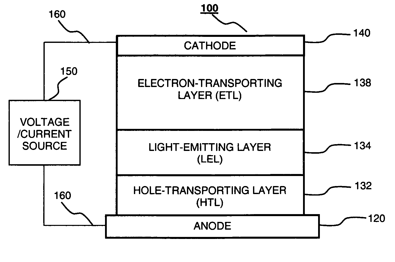
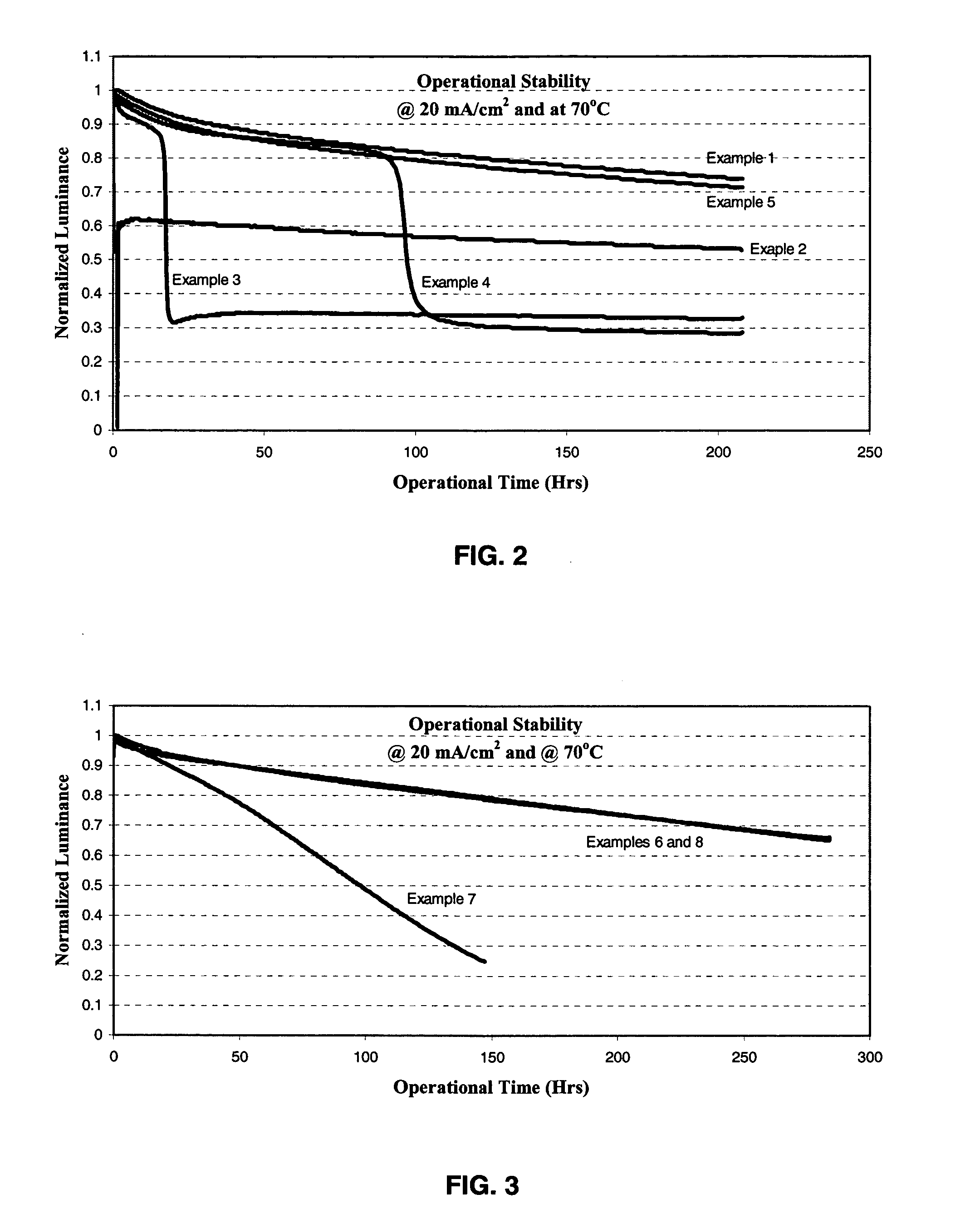
[0124] An OLED was constructed in the manner described in Example 1, except in Step (3) wherein the 40-nm-thick Alq ETL is now replaced by a 40-nm-thick Bphen ETL which contains Alq, 10% by volume, as a crystallization-inhibitor. The completed device structure is denoted as ITO / CFx / NPB(90) / Alq(20) / Bphen:Alq(10%)(40) / MgAg. The EL performance of the device, measured at a current density of 20 mA / cm2, is shown in Table I, wherein the drive voltage, luminance, luminous efficiency, power efficiency, EL peak, and the T70(70° C.) are listed. The normalized luminance vs. operational time is shown in FIG. 2.
example 4 (
Inventive Example)
[0125] An OLED was constructed in the manner described in Example 1, except in Step (3) wherein the 40-nm-thick Alq ETL is now replaced by a 40-nm-thick Bphen ETL which contains Alq, 20% by volume, as a crystallization-inhibitor. The completed device structure is denoted as ITO / CFx / NPB(90) / Alq(20) / Bphen:Alq(20%)(40) / MgAg. The EL performance of the device, measured at a current density of 20 mA / cm2, is shown in Table I, wherein the drive voltage, luminance, luminous efficiency, power efficiency, EL peak, and the T70(70° C.) are listed. The normalized luminance vs. operational time is shown in FIG. 2.
example 5 (
Inventive Example)
[0126] An OLED was constructed in the manner described in Example 1, except in Step (3) wherein the 40-nm-thick Alq ETL is now replaced with a 40-nm-thick Bphen ETL which contains Alq, 30% by volume, as a crystallization-inhibitor. The completed device structure is denoted as ITO / CFx / NPB(90) / Alq(20) / Bphen:Alq(30%)(40) / MgAg. The EL performance of the device, measured at a current density of 20 mA / cm2, is shown in Table I, wherein the drive voltage, luminance, luminous efficiency, power efficiency, EL peak, and the T70(70° C.) are listed. The normalized luminance vs. operational time is shown in FIG. 2.
TABLE IExample(Type)LuminousPower(EL measuredVoltageLuminanceEfficiencyEfficiencyEL PeakT70(70° C.)@ 20 mA / cm2)(V)(cd / m2)(cd / A)(lm / W)(nm)(Hrs)1 (Comparative)6.935092.541.15524>2002 (Comparative)6.636353.181.505243 (Inventive)5.715972.981.64524174 (Inventive)6.165993.001.53524905 (Inventive)6.035722.861.49524>200
[0127] From the data shown in both Table I and FIG. 2, i...
PUM
| Property | Measurement | Unit |
|---|---|---|
| Tg | aaaaa | aaaaa |
| Tg | aaaaa | aaaaa |
| optical energy band gap | aaaaa | aaaaa |
Abstract
Description
Claims
Application Information