Semiconductor device using semiconductor chip

a semiconductor chip and semiconductor technology, applied in semiconductor devices, semiconductor/solid-state device details, electrical devices, etc., can solve the problems of increasing the inability to orient each corner in a predetermined direction, etc., to reduce the positional deviation of the semiconductor chip, reduce the size and weight of the semiconductor device, and reduce the width and the length of the semiconductor device.

Inactive Publication Date: 2005-07-21
ROHM CO LTD
View PDF4 Cites 69 Cited by
  • Summary
  • Abstract
  • Description
  • Claims
  • Application Information

AI Technical Summary

Benefits of technology

[0025] By the subsequent hardening of the melted die bonding material by cooling, the semiconductor chip is bonded at or near the center of the die pad connected to one of the electrode terminals, with one of the corners of the semiconductor chip oriented toward the narrow patterned conductor connected to the die pad so that each of the corners is constantly oriented in a predetermined direction. Therefore, it is possible to reduce the positional deviation of the semiconductor chip from the center of the die pad and the deviation of the corner orientation of the semiconductor chip.
[0026] As a result, the possibility of a connection failure, which may occur in electrically connecting the semiconductor chip to one of the electrode terminals by wire bonding using a metal wire, is reliably reduced. Further, when the semiconductor chip is to be packaged with a molded portion made of a synthetic resin, the molded portion can be made smaller by as much as the above two kinds of deviation is reduced, whereby the size and weight of the semiconductor device can be reduced.
[0027] As noted above, the self alignment to locate the semiconductor chip at or near the center of the die pad and to orient the semiconductor chip so that one of the corners is oriented toward the narrow patterned conductor can be reliably achieved by making the diameter of the die pad 0.6 to 1.5 times the diagonal dimension of the semiconductor chip.
[0028] In the second aspect, the die pad may be arranged between the paired electrode terminals arranged on a generally straight line, and the narrow patterned conductor may be arranged to extend from the

Problems solved by technology

Conventionally, although the die pad has a rectangular configuration which is similar to the rectangular configuration of the semiconductor chip, the die pad is made considerably larger than the semiconductor chip to be bonded thereto, which causes the problems described below.
However, since the semiconductor chip floated on the melted die bonding material can rotate freely, each of the corners cannot be oriented in a predetermined direction.
The positional deviation from the center and deviation of the corner orientation of the semiconductor chip may hinder the connecti

Method used


Image

  • Semiconductor device using semiconductor chip
  • Semiconductor device using semiconductor chip
  • Semiconductor device using semiconductor chip

Examples


first embodiment

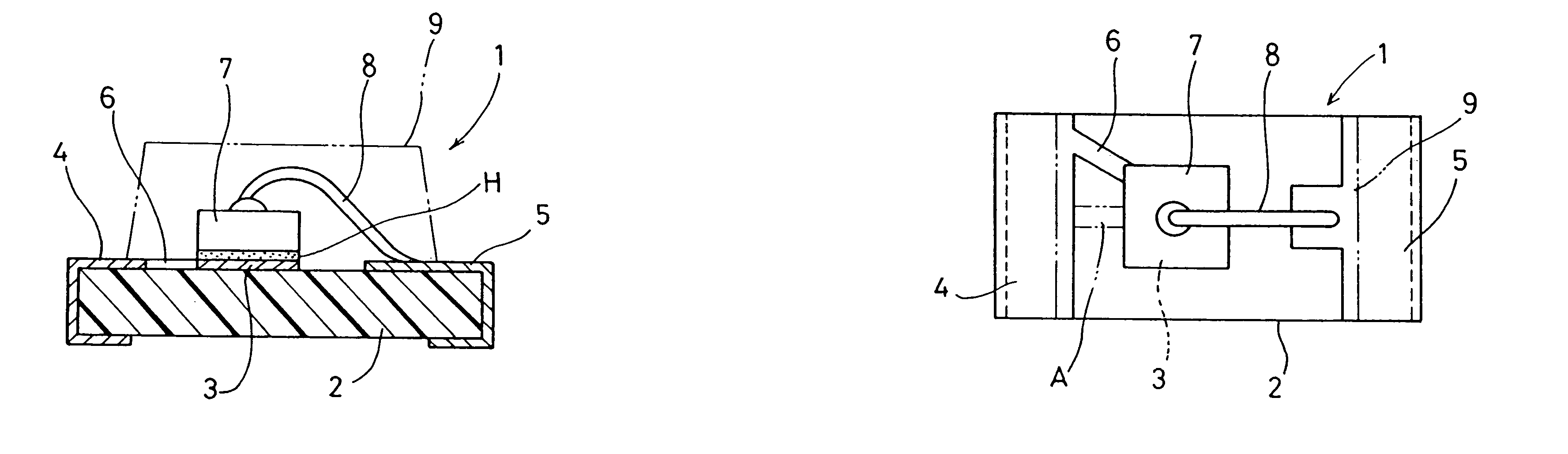
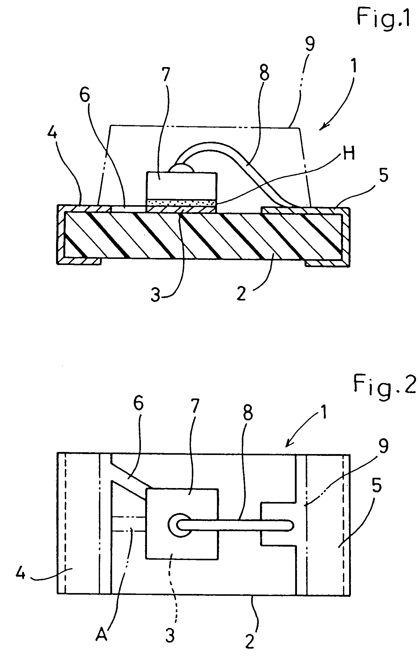
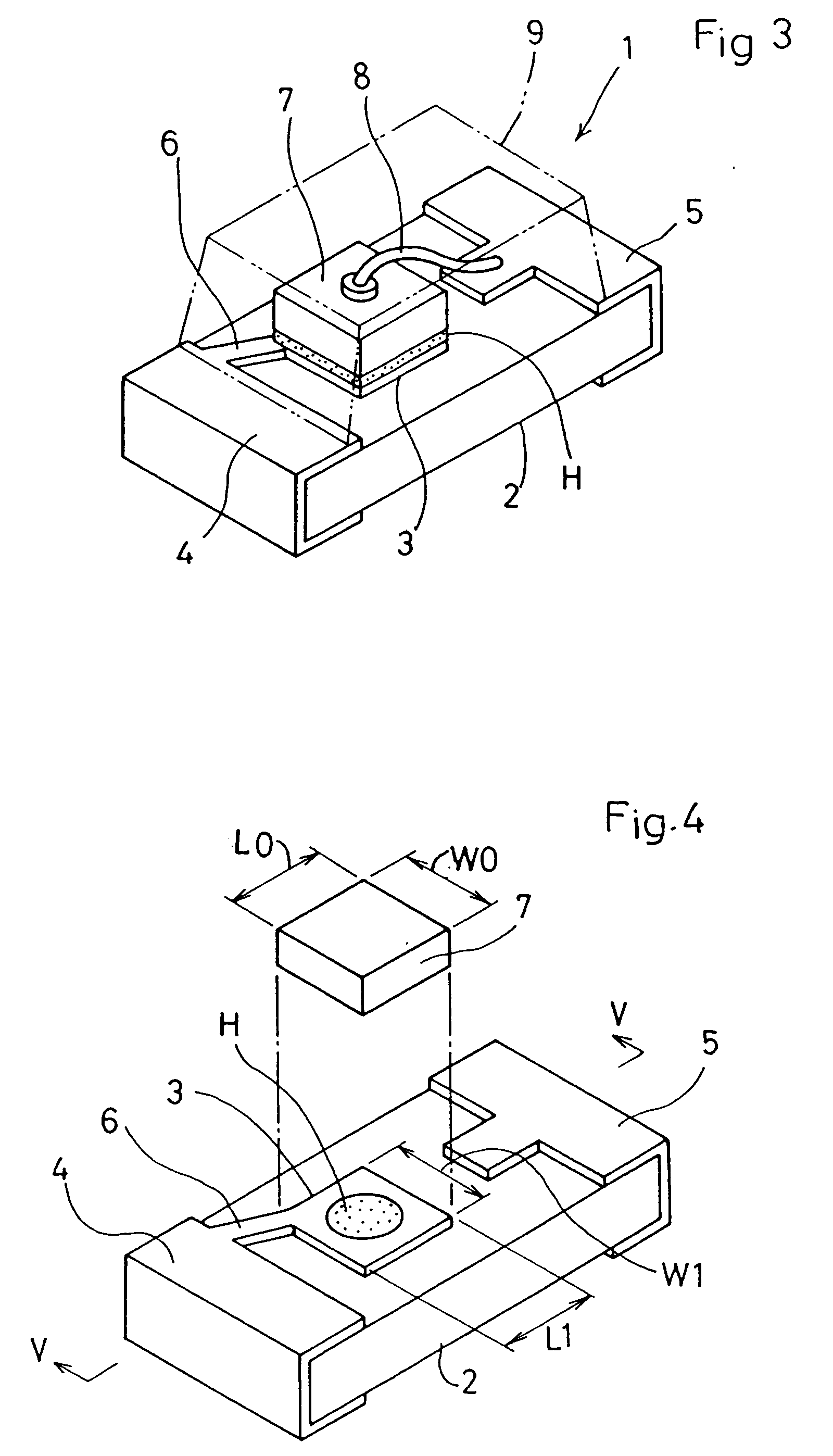
[0060]FIGS. 1-7 show the present invention.

[0061] Indicated by the reference sign 1 in these figures is a chip-type LED device as an embodiment of semiconductor device.

[0062] The chip-type LED device 1 includes an insulating substrate 2 in the form of a chip. The insulating substrate 2 has an upper surface formed with a rectangular die pad 3 and a pair of terminal electrodes 4, 5 all of which are made of a metal film, and a narrow patterned conductor 6 made of a metal film and electrically connecting the terminal electrode 4 to the die pad 3.

[0063] The chip-type LED device 1 further includes an LED chip 7 bonded to the upper surface of the die pad 3, a thin metal wire 8 connecting the LED chip 7 and the terminal electrode 5 by wire bonding, and a molded portion 9 made of a light-permeable synthetic resin such as a transparent resin for packaging the LED chip 6 and the wiring pattern 6.

[0064] The paired terminal electrodes 4, 5 extend from the upper surface onto an end surface and...

second embodiment

[0080]FIGS. 13-19 show the present invention.

[0081] Indicated by the reference sign 11 in these figures is a chip-type LED device. The chip-type LED device 11 includes an insulating substrate 12 in the form of a chip. The insulating substrate 12 has an upper surface formed with a die pad 13 made of a metal film to have a circular configuration with a diameter D, and a pair of terminal electrodes 14 and 15 made of a metal film and provided on opposite sides of the die pad. The upper surface of the insulating substrate 12 is further formed with a narrow patterned conductor 16 made of a metal film and electrically connecting the terminal electrode 14 to the die pad 13.

[0082] The chip-type LED device 11 further includes an LED chip 17 bonded to the upper surface of the die pad 13, a thin metal wire 18 connecting an electrode on the upper surface of the LED chip 17 to the terminal electrode 15 by wire bonding, and a molded portion 19 made of a light-permeable synthetic resin such as a t...

third embodiment

[0098]FIGS. 21 and 22 show the present invention.

[0099] In the chip-type LED device 21 according to the third embodiment, instead of the paired electrode terminals and the die pad all of which comprise a metal film formed on an insulating substrate, a pair of electrode terminals and a die pad all of which comprise a relatively thick metal plate are provided, and the insulating substrate is not used.

[0100] Specifically, both of the electrode terminal 25 and the electrode terminal 24 connected to the circular die pad 23 via a narrow patterned conductor 26 are made of a metal plate. Similarly to the foregoing embodiments, an LED chip 27 is bonded on the upper surface of the die pad 23 with solder paste H, and an electrode on the LED chip 27 is connected to the electrode terminal 25 by wire bonding using a metal wire 28. The LED chip 27, the narrow patterned conductor 26 and the metal wire 28 are packaged with a molded portion 29 made of a light-permeable synthetic resin such as a tran...


PUM


Abstract

A semiconductor device includes an insulating substrate 2 having an obverse surface formed with a die pad 3, a rectangular semiconductor chip 7 such as an LED chip bonded to the die pad with a die bonding material 10, and a molded portion 9 made of a synthetic resin for packaging the semiconductor chip. The die pad 3 may be rectangular with dimensions close to those of the semiconductor chip or circular with a diameter close to the diagonal dimension of the semiconductor chip, whereby the positioning and orienting of the semiconductor chip can be accurately performed in bonding the semiconductor chip.

Description

BACKGROUND OF THE INVENTION [0001] 1. Field of the Invention [0002] The present invention relates to a semiconductor device using a semiconductor chip, and particularly to a semiconductor device including a semiconductor chip bonded to a die pad and packaged with a molded portion made of a synthetic resin. [0003] 2. Description of the Related Arts [0004] Generally, a light emitting diode lamp of the type described above includes an insulating substrate in the form of a chip, on which a die pad and a pair of first and second electrode terminals all of which are made of a metal film are formed so that the die pad is electrically connected to the first electrode terminal. The device further includes a semiconductor chip bonded to the die pad and electrically connected to the second electrode terminal. [0005] To bond the semiconductor chip to the die pad electrically connected to the first electrode terminal in the semiconductor device, a thermally meltable die bonding material such as ...

Claims


Application Information

Patent Timeline
IPC IPC(8): H01L23/498H01L33/38H01L33/48H01L33/62
CPCH01L23/49838H01L24/32H01L2224/48247H01L2224/32245H01L2224/27013H01L2924/12041H01L24/29H01L2924/014H01L2924/01033H01L2924/01023H01L2924/01006H01L2924/01005H01L24/48H01L2224/83385H01L2924/01082H01L2924/01078H01L2924/0105H01L2224/92247H01L2224/83192H01L2224/73265H01L2224/48465H01L2224/48227H01L24/83H01L33/38H01L33/486H01L33/62H01L2224/32225H01L2224/48091H01L2924/00014H01L2924/00012H01L2924/00H01L24/73H01L2224/451H01L2224/83143H01L2924/181H01L2924/00015H01L2224/05599H01L2224/45099H01L2224/45015H01L2924/207
Inventor ISOKAWA, SHINJIYAMAGUCHI, TOMOJI
Owner ROHM CO LTD
Why Eureka
Try Eureka