Partially populated ball grid design to accommodate landing pads close to the die

a ball grid and die-nahing technology, applied in the field of semiconductor packages, can solve the problems of too long wires, inability to accommodate landing pads, and inability to allow miniaturized spacing for wire landing pads, so as to reduce the length of critical electrical connections

Inactive Publication Date: 2005-07-21
DIALOG SEMICONDUCTOR GMBH
View PDF8 Cites 9 Cited by
  • Summary
  • Abstract
  • Description
  • Claims
  • Application Information

AI Technical Summary

Benefits of technology

[0012] A principal object of the present invention is to define a method and a structure to reduce the length of critical electrical connections, e.g. carrying high current signals, high speed signals or radio frequency signals, of a semiconductor package between a semiconductor chip and the related landing pads of said wires on a package substrate without increasing the space required for the semiconductor package.
[0014] In accordance with the objects of this invention a method to reduce the length of critical electrical connections of a semiconductor package between bond pads on semiconductor chips and landing pads on a multi-chip substrate has been achieved. Said method is comprising, first, providing more than one semiconductor chip, a grid array semiconductor package substrate, electrical connections from said semiconductor substrate to external circuitry performed in a grid array and electrical connections between said chip and said substrate. The steps of said method comprise further to identify critical wires requiring landing pads within said grid array due to bond wire-length limitations, to identify non-critical wires which can have landing pads outside said grid array, to design a grid array creating empty locations within said grid array as required and identified in the previous steps for landing pads of critical wires, and to design the leads from the landing pads of said critical wires to the next suitable via hole.
[0015] In accordance with the objects of this invention a structure to reduce the length of critical electrical connections of a semiconductor package between a semiconductor-chip and a single-chip substrate has been achieved. Said structure comprises a semiconductor chip having bonding pads for electrical connections to landing pads on a substrate where said chip is mounted on, a means of electrical connections between said semiconductor chip and said substrate wherein landing pads on said substrate are provided for said electrical connections, and a substrate said semiconductor chip is mounted on being electrically connected to said chip and to an external circuitry wherein said electrical connections to an external circuit are performed by a grid array arrangement and wherein said landing pads for connections requiring very a limited length are located within said grid array.
[0016] In accordance with the objects of this invention a structure to reduce the length of critical electrical connections of a semiconductor package between semiconductor chips and a multi-chip substrate has been achieved. Said structure is comprising more than one semiconductor chip all having landing pads for electrical connections to a substrate where said chips are mounted on, a means of electrical connections between said semiconductor chips and said substrate wherein landing pads on said substrate are provided for said electrical connection, and a substrate said semiconductor chips are mounted on being electrically connected to said chips and to an external circuitry wherein said electrical connections to an external circuit are performed by an grid array arrangement and wherein said landing pads for connections requiring very a limited length are located within said grid array.

Problems solved by technology

With the general trend of miniaturization the length of said wires between the semiconductor chip and the substrate is causing more and more problems to the designers, especially for high current signals.
The miniaturized spacing does not allow for wire landing pads in the via / ball array.
This causes problems with wires being too long.
The disadvantage of this solution is that the grid array has been moved more far away from the semiconductor die and the package is consuming additional space on the motherboard and hence is too expensive.
With the progress of miniaturization of semiconductor chips it is a growing challenge for the designers of electronic circuits to find a solution having short wires consuming minimal space on the motherboard.

Method used


Image

  • Partially populated ball grid design to accommodate landing pads close to the die
  • Partially populated ball grid design to accommodate landing pads close to the die
  • Partially populated ball grid design to accommodate landing pads close to the die

Examples


Embodiment Construction

[0023] The preferred embodiments disclose a method and a structure capable to reduce the wire-lengths of the wires providing the connections of a semiconductor package from a chip to a substrate without increasing the space required on a motherboard.

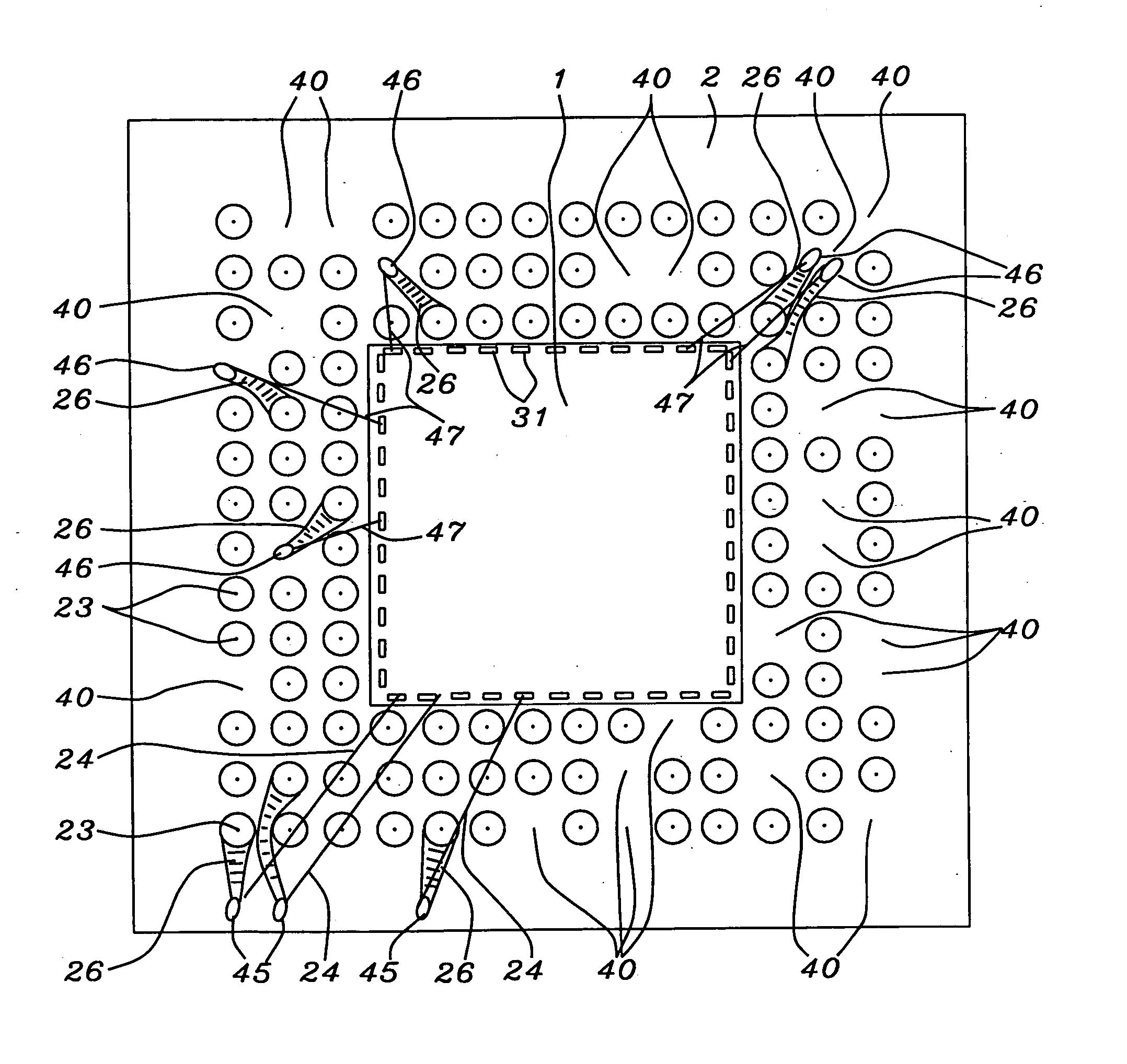
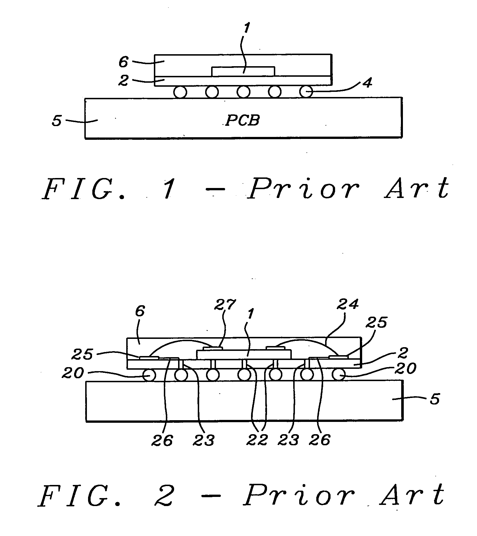
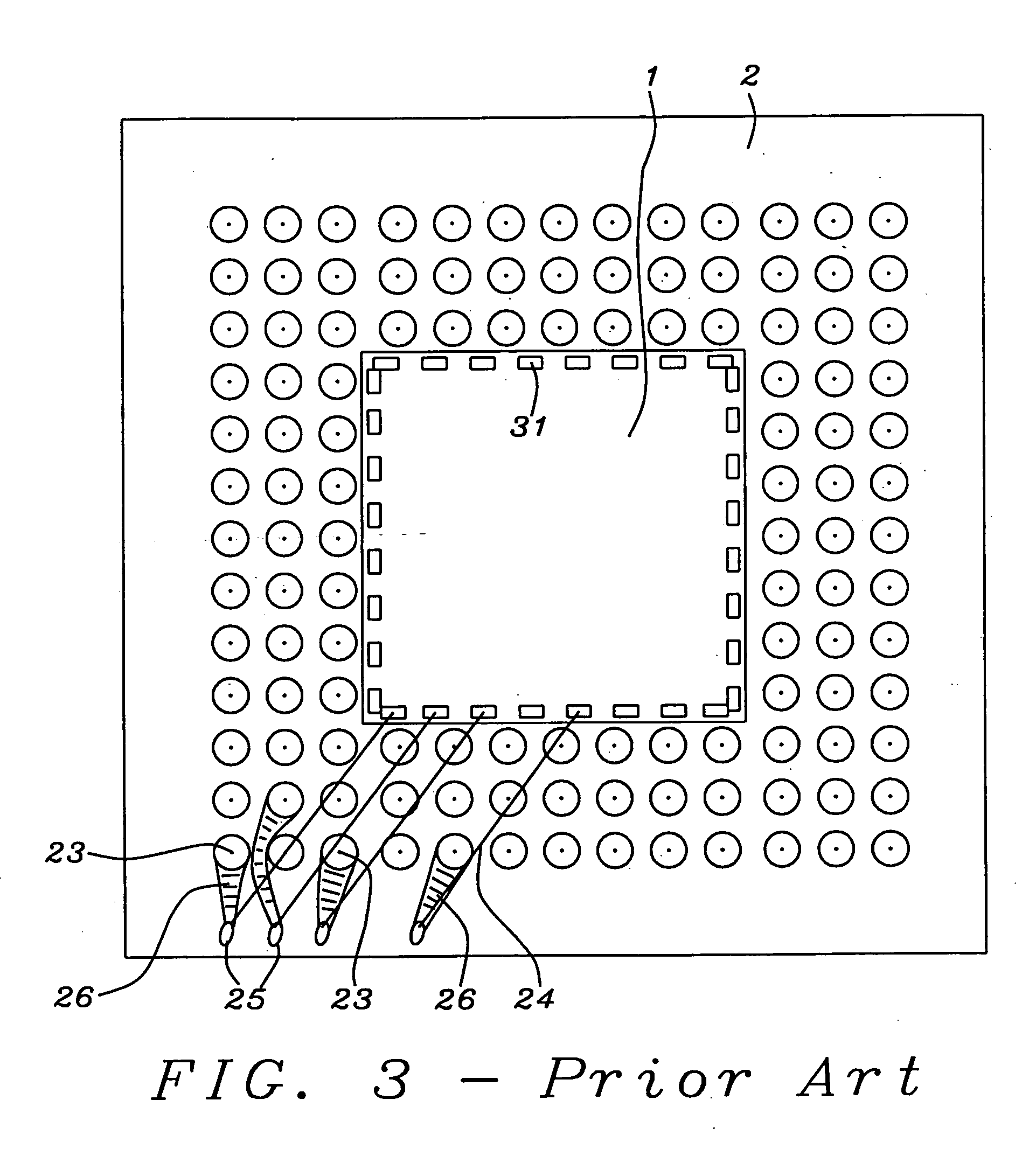
[0024] The BGA design principles allow any number of solder balls or rows of solder balls. FIG. 4 shows a principal layout of a new structure of the present invention. Similar to FIG. 3 prior art, FIG. 4 shows a chip 1 on a substrate 2, leads 26 from wire landing pads to through-hole vias 23 and wires 24 from said landing pads on the substrate 2 to bonding pads 31 on the chip 1. In order to reduce the complexity in FIG. 4 only a few wire-landing pads, related bonding wires, and leads on the substrate are shown. One of the objectives of the invention was not to increase the number of solder balls required and not to increase the size of the area required on the mother-board, thus not increasing the cost of said BGA module. In the design ...


PUM


Abstract

Methods and structures to reduce in semiconductor packages the length of critical electrical connections between bond pads on one or multiple semiconductor chips and wire landing pads on a substrate have been achieved. An electrical connection becomes critical if high current, high speed or radio frequency signals have to be transported. Moving the wire landing pads of critical connections on the substrate closer to the semiconductor chip utilizing unpopulated spaces of an array grid design reduces the length of said wires. This could be a ball grid array (BGA) or any other kind of grid array. Said methods and structures invented are applicable to single-chip modules and to multi-chip modules. The design of the grid array has to be modified to provide free spaces for the wire landing pads of critical electrical connections within the grid array close to the semiconductor chip as required by the design rules. The design change can be done without increasing the number of solder balls or solder pins, etc. and without increasing the area required on the motherboard.

Description

BACKGROUND OF THE INVENTION [0001] (1) Field of the Invention [0002] This invention relates generally to semiconductor packages, and more particular, to electrical connections between semiconductor dies and the related substrate as part of the package. [0003] (2) Description of the Prior Art [0004] The present miniaturization trend in electronics towards higher-performance, smaller and lighter products has resulted in an increasing demand for smaller component packages and / or higher pin counts. The Ball Grid Array (BGA) concept has received much appreciation owing to its inherent, potential benefits to surface mount production. The BGA, taking advantage of the area under the package for the solder sphere interconnections, accommodates the increasing number of I / Os needed. [0005]FIG. 1 prior art shows how a BGA package is composed of a chip 1, a BGA substrate 2, an interconnection 4 between said substrate 2 to a Printed Circuit Board (PCB) or motherboard 5 and a cover 6 to seal said ...

Claims


Application Information

Patent Timeline
Patent Type & Authority Applications(United States)
IPC IPC(8): H01L23/498
CPCH01L23/49838H01L24/48H01L24/49H01L2224/45124H01L2224/45144H01L2224/45147H01L2224/48091H01L2224/49171H01L2924/01013H01L2924/01029H01L2924/01079H01L2924/14H01L2924/15183H01L2924/15311H01L2224/48227H01L2924/014H01L2924/01076H01L24/45H01L2924/00014H01L2924/00H01L2224/05553H01L2224/45015H01L2924/10162H01L2924/181H01L2924/00012
Inventor VONSTAUDT, HANS MARTIN
Owner DIALOG SEMICONDUCTOR GMBH
Why Eureka
Try Eureka