Memory control device and memory control method

a memory control device and control method technology, applied in the direction of memory adressing/allocation/relocation, instruments, sustainable buildings, etc., can solve the problems of power noise, signal consumption, power noise, etc., to prevent delay of access operation, reduce noise, and avoid overhead time for refresh operation

Active Publication Date: 2005-07-21
SOCIONEXT INC
View PDF2 Cites 16 Cited by
  • Summary
  • Abstract
  • Description
  • Claims
  • Application Information

AI Technical Summary

Benefits of technology

[0017] Thereby, a refresh command and a refresh address required for a refresh operation of the synchronous-type semiconductor memory device are supplied from the memory control device and the number of sense amplifiers to be activated concurrently can be designated from the memory control device side. Therefore, a peak value of noises can be reduced by designating reduced number of sense amplifiers to be activated concurrently. Furthermore, even if the number of sense amplifiers to be activated concurrently is reduced to lower a peak value of noises while refresh frequency increases, the synchronous-type semiconductor memory device is controlled to conduct a data input / output access operation and a refresh operation in parallel. Therefore, overhead time for a refresh operation is not increased and delay of an access operation can be prevented.

Problems solved by technology

Since an unnecessary clock signal is supplied during input / output of image data in which synchronous operation with the aid of a clock signal is not required for input / output operation, operational current due to operation at the internal circuit and charge / discharge current to wiring capacity held by clock a signal are consumed and power noises occur.
As the number of sense amplifiers to be activated concurrently is larger, a peak value of current consumed by an SDRAM and a peak value of power noise become larger.
Therefore, there arise fears such that data destruction occurs at an SDRAM and erroneous operation is likely to occur at each chip in case plural chips are built in a single package.
Therefore, the memory control device cannot change the number of sense amplifiers to be activated concurrently, which is a problem.
As a result, overhead time for refresh is increased and access operation gets slow, which is a problem.

Method used


Image

  • Memory control device and memory control method
  • Memory control device and memory control method
  • Memory control device and memory control method

Examples


Embodiment Construction

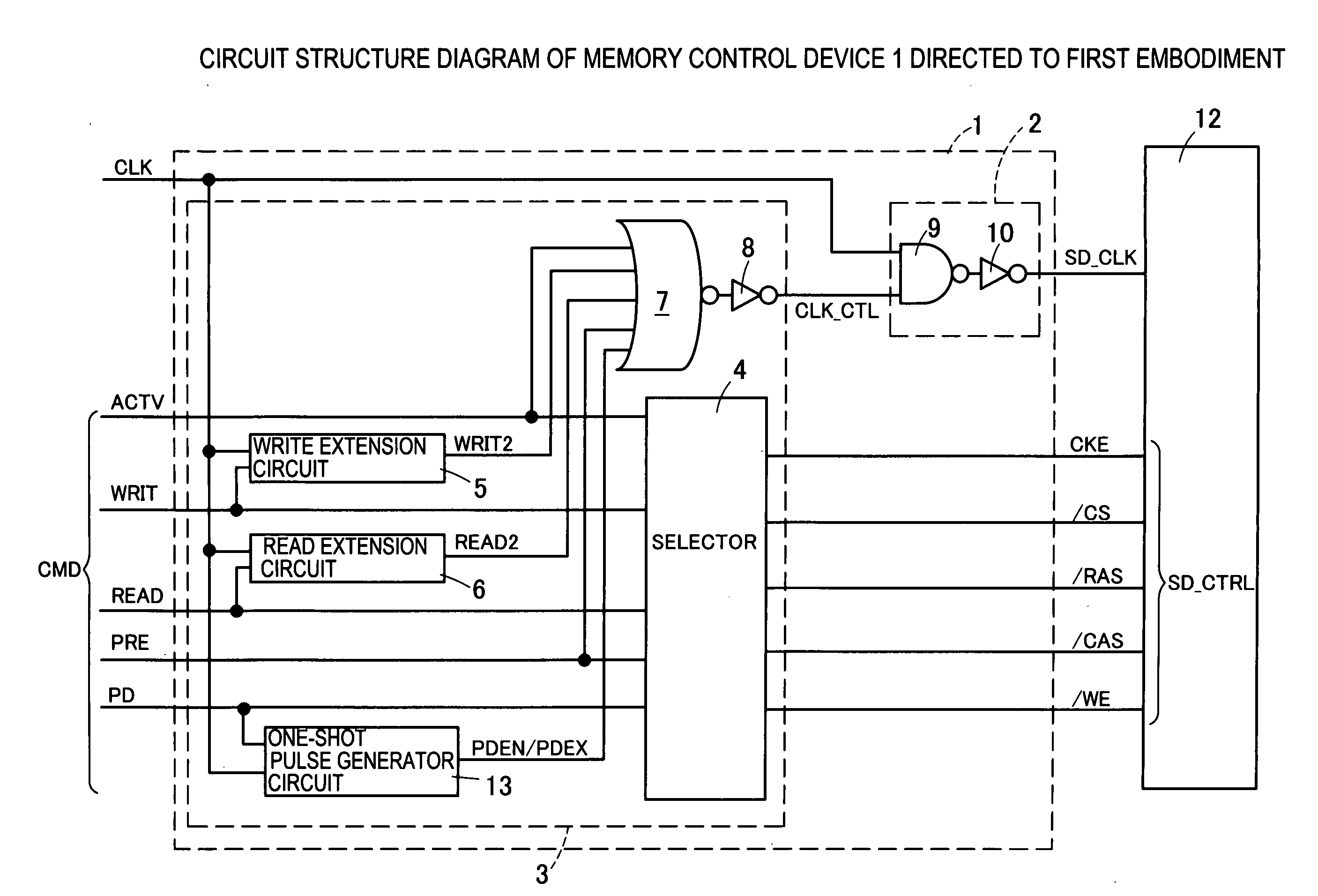
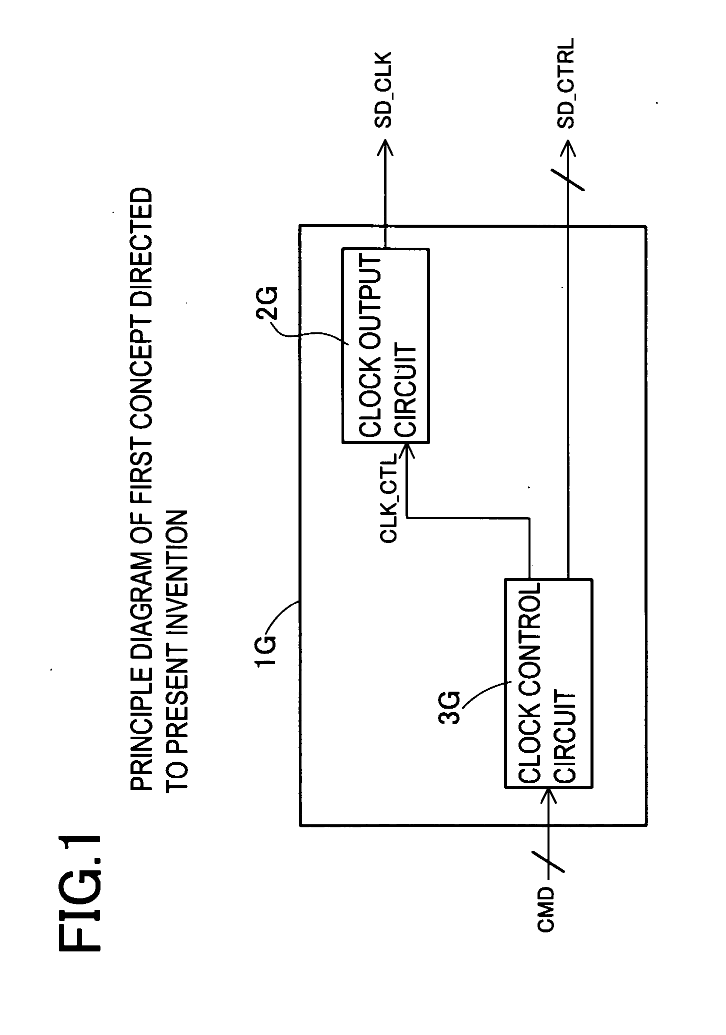
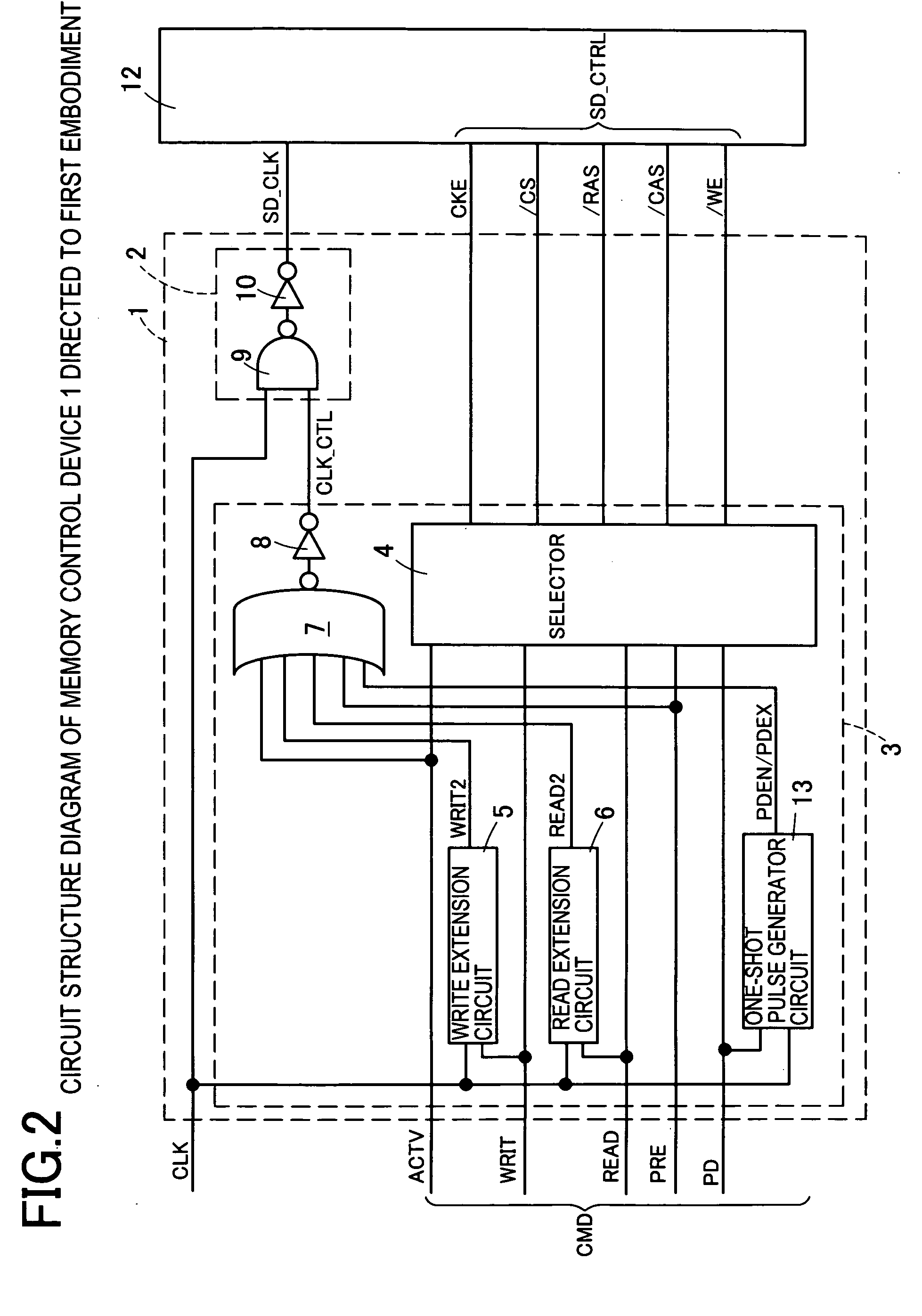
[0041] Preferred embodiments of a memory control device and memory control method directed to the present invention will be described in detail below with reference to FIG. 1 through FIG. 20. FIG. 1 shows a principle diagram of first concept. A memory control device 1G is equipped with a clock output circuit 2G and a clock control circuit 3G. Upon receipt of an external command CMD to be inputted to the memory control device 1G, the clock control circuit 3G outputs a clock inform signal CLK_CTL, in response to the external command CMD, to the clock output circuit 2G. The clock control circuit 3G also outputs a control signal SD_CTRL to a synchronous-type semiconductor memory device (not shown). When a clock inform signal CLK_CTL is inputted to the clock output circuit 2G, a control clock SD_CLK is outputted to the synchronous-type semiconductor memory device in response to the clock inform signal CLK_CTL. Thereby, the clock output circuit 2G outputs a control clock SD_CLK just durin...


PUM


Abstract

It is intended to provide a memory control device and memory control method capable of reducing charge/discharge current consumed while various commands are inputted to a semiconductor memory device and reducing occurrence of power noises. During periods TT1, TT2, and TT3 which are parts of a period tCKE in which a clock enable signal CKE is in active state, supply of a control clock SD_CLK from a memory control device 1 to a synchronous-type semiconductor memory device 12 can be stopped. Furthermore, in case an input of a data input/output period of an external command and that of refresh operation period of a refresh command RCMD overlap and an access region of the external command and that of the refresh command RCMD do not coincide, those commands are converted to control command signal SD_CMD in parallel, whereby parallel conversion processing operation can be conducted.

Description

CROSS-REFERENCE TO RELATED APPLICATIONS [0001] This application is based upon and claims the benefit of priority from each of the prior Japanese Patent Application No. 2004-011856 filed on Jan. 20, 2004, the entire contents of which are incorporated herein by reference. BACKGROUND OF THE INVENTION [0002] 1. Field of the Invention [0003] The present invention relates to a memory control device and memory control method capable of reducing charge / discharge current consumed during inputs of various commands to a semiconductor memory device and reducing occurrence of power noises. [0004] 2. Description of Related Art [0005] Due to miniaturization of portable electric appliances of these days, there have increased the number of multi-chip-package-type semiconductor devices and that of system-in-package-type semiconductor devices wherein plural chips are built in a single package. Since plural chips are built in a single package, heat and power noises occur at the plural chips. [0006] For...

Claims


Application Information

Patent Timeline
Patent Type & Authority Applications(United States)
IPC IPC(8): G06F12/00G06F12/02G06F13/42G11C8/00G11C11/406
CPCG06F13/4243Y02B60/1235Y02B60/1228G11C11/406Y02D10/00
Inventor KATO, YOSHIHARUTSUKISHIRO, GENTAKEMAE, YOSHIHIRO
Owner SOCIONEXT INC
Why Eureka
Try Eureka