Integrated photonic devices
a photonic device and integrated technology, applied in the field of photonic devices, can solve the problems of high cost, high cost, and inability to meet the requirements of high-efficiency coupling, and achieve the effect of high-efficiency coupling
- Summary
- Abstract
- Description
- Claims
- Application Information
AI Technical Summary
Benefits of technology
Problems solved by technology
Method used
Image
Examples
first embodiment
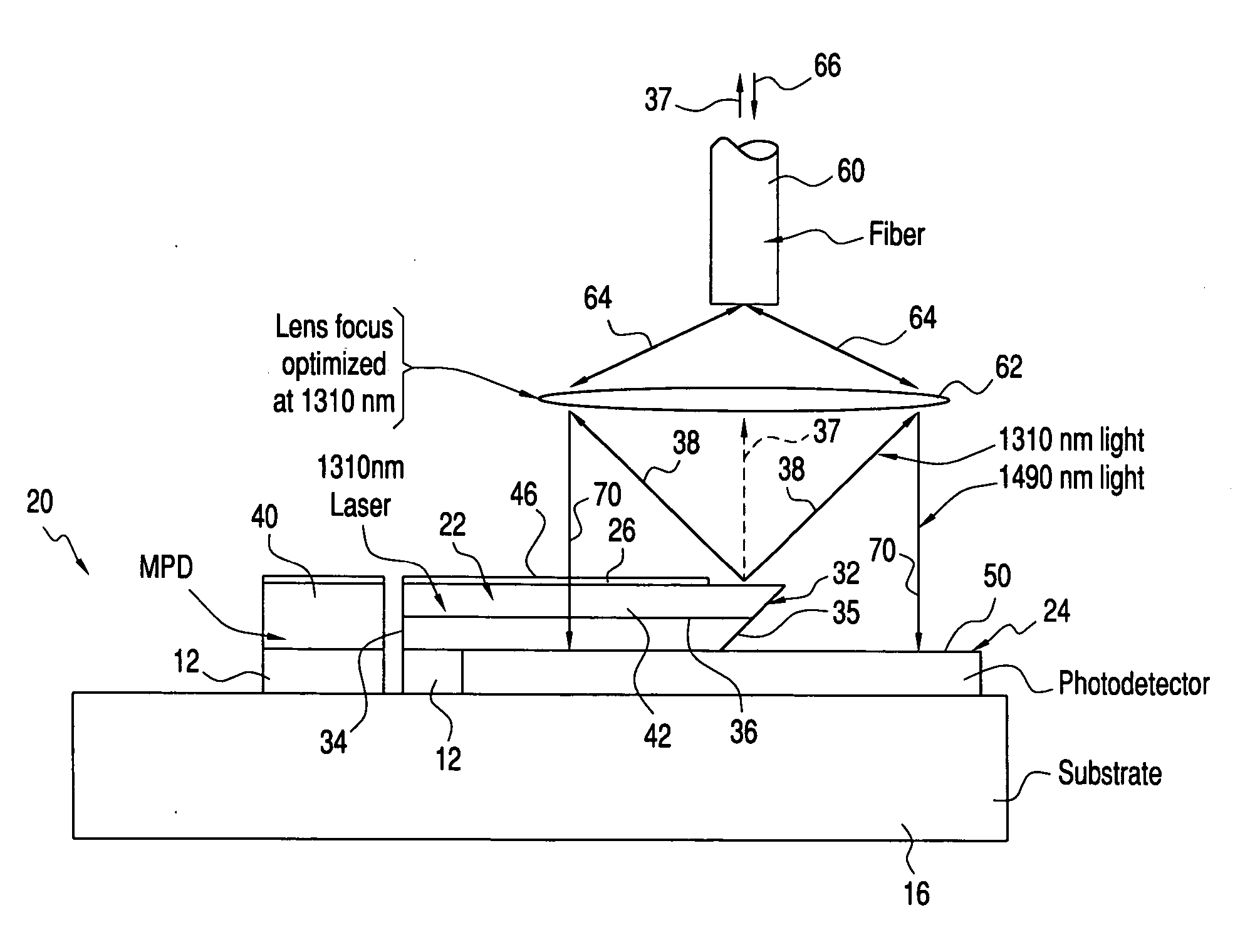
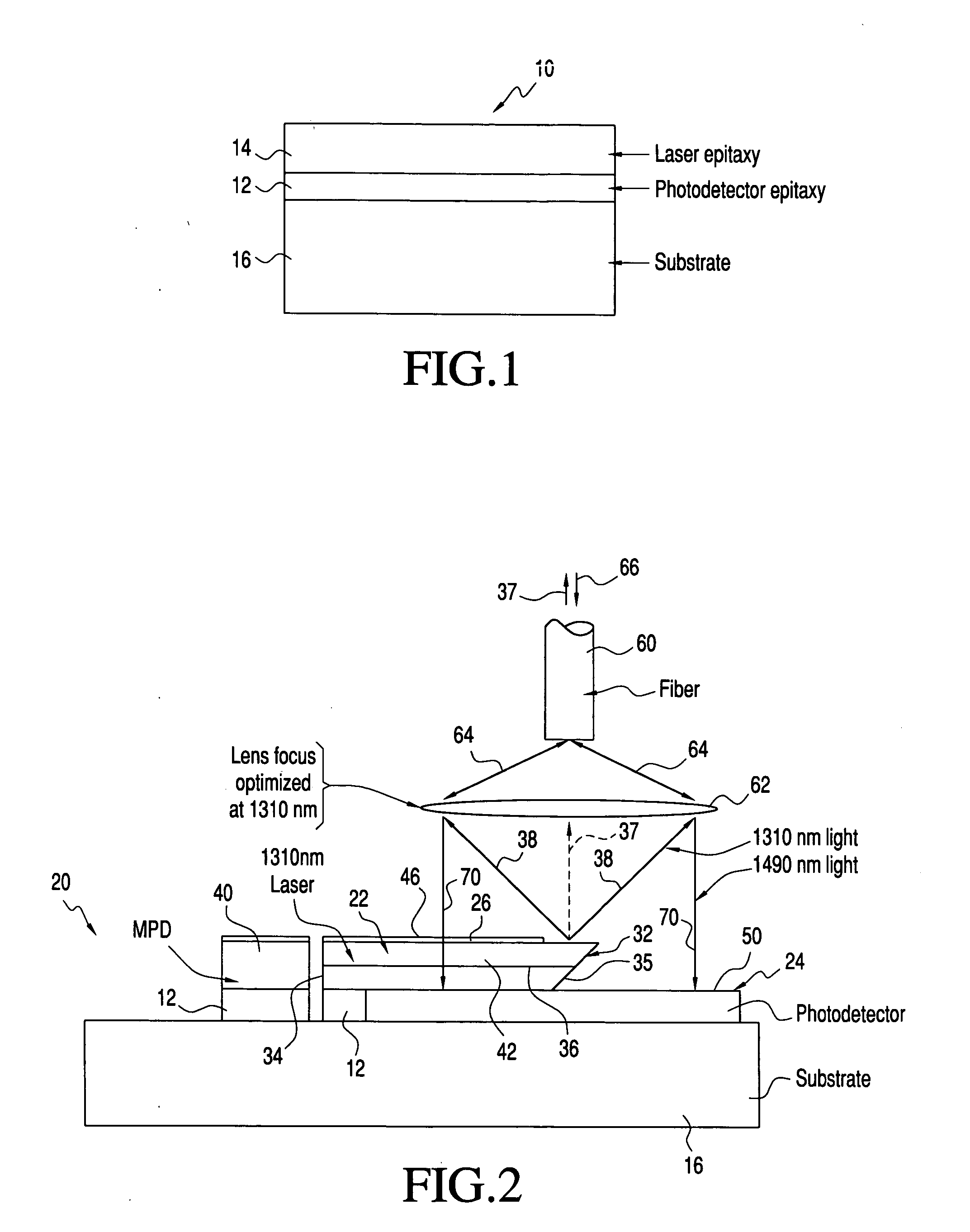
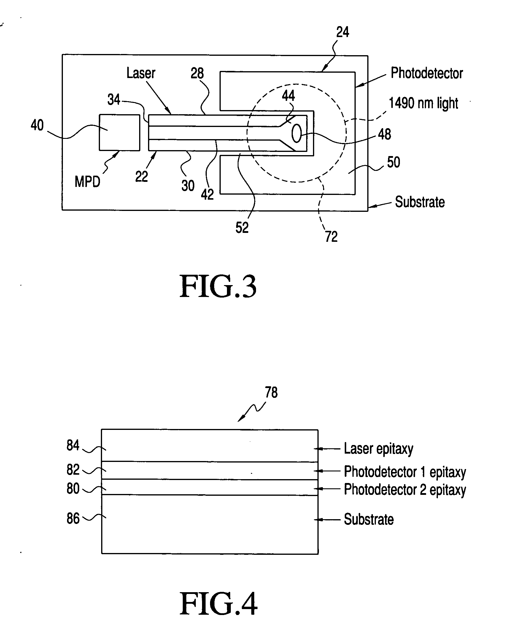
[0031] In the invention, illustrated in FIGS. 2 and 3, a monolithic photonic device, or chip 20 incorporates an integral laser 22 and an integral detector 24 fabricated in separate mesas in respective structures 12 and 14 of the chip 10. The laser 22 is formed in structure 14 by a conventional masking and etching technique to produce, for example, an elongated, horizontal ridge-type optical cavity having a top surface 26, mesa side walls 28 and 30, and first and second ends 32 and 34. An angled totally internally reflective facet 35 is formed at the first end 32 to direct output light propagated in the laser upwardly out of the cavity through a top emissive surface, while the second end 34 of the cavity is formed by a vertical, totally internally reflective facet to permit lasing in the optical cavity. The angled facet 35 at end 32 is fabricated by etching the structure 14 downwardly and inwardly at or near a 45° angle with respect to the top surface 26, and causes light generated i...
second embodiment
[0035] the invention is illustrated in FIG. 4, wherein a chip 78 includes three epitaxial structures, detectors 80 and 82 and laser 84, which are fabricated on a substrate 86. Those semiconductor structures may share common layers to facilitate the fabrication of the device. For example, a highly doped semiconductor layer can be introduced between detector layers 80 and 82 to provide a ground plane to improve electrical isolation and high-speed performance.
[0036] A monolithically integrated photonic device 90, illustrated in FIG. 5, may be fabricated from chip 78 in the manner described above with respect to the device of FIGS. 2 and 3. In this case, a laser 92 is fabricated, as by masking and etching, in laser structure 84, with the etching forming a trench, similar to the trench 52 of FIG. 3, extending downwardly through both detector structures 80 and 82 to the top of substrate 86, so that the laser and the surrounding detectors are located on separate mesas. The laser is etched ...
PUM
 Abstract
Description
Claims
Application Information


