Method of manufacturing semiconductor device

a manufacturing method and semiconductor technology, applied in semiconductor devices, semiconductor/solid-state device details, electrical devices, etc., can solve the problems of increasing the amount of vapor deposition, and increasing the amount of warping of the wafer, so as to prevent plating and small variation in film thickness

a manufacturing method and semiconductor technology, applied in semiconductor devices, semiconductor/solid-state device details, electrical devices, etc., can solve the problems of increasing the amount of vapor deposition, and increasing the amount of warping of the wafer, so as to prevent plating and small variation in film thickness

US20050158979A1Active Publication Date: 2005-07-21FUJI ELECTRIC CO LTD

Image

  • Method of manufacturing semiconductor device
  • Method of manufacturing semiconductor device
  • Method of manufacturing semiconductor device

Examples


Embodiment Construction

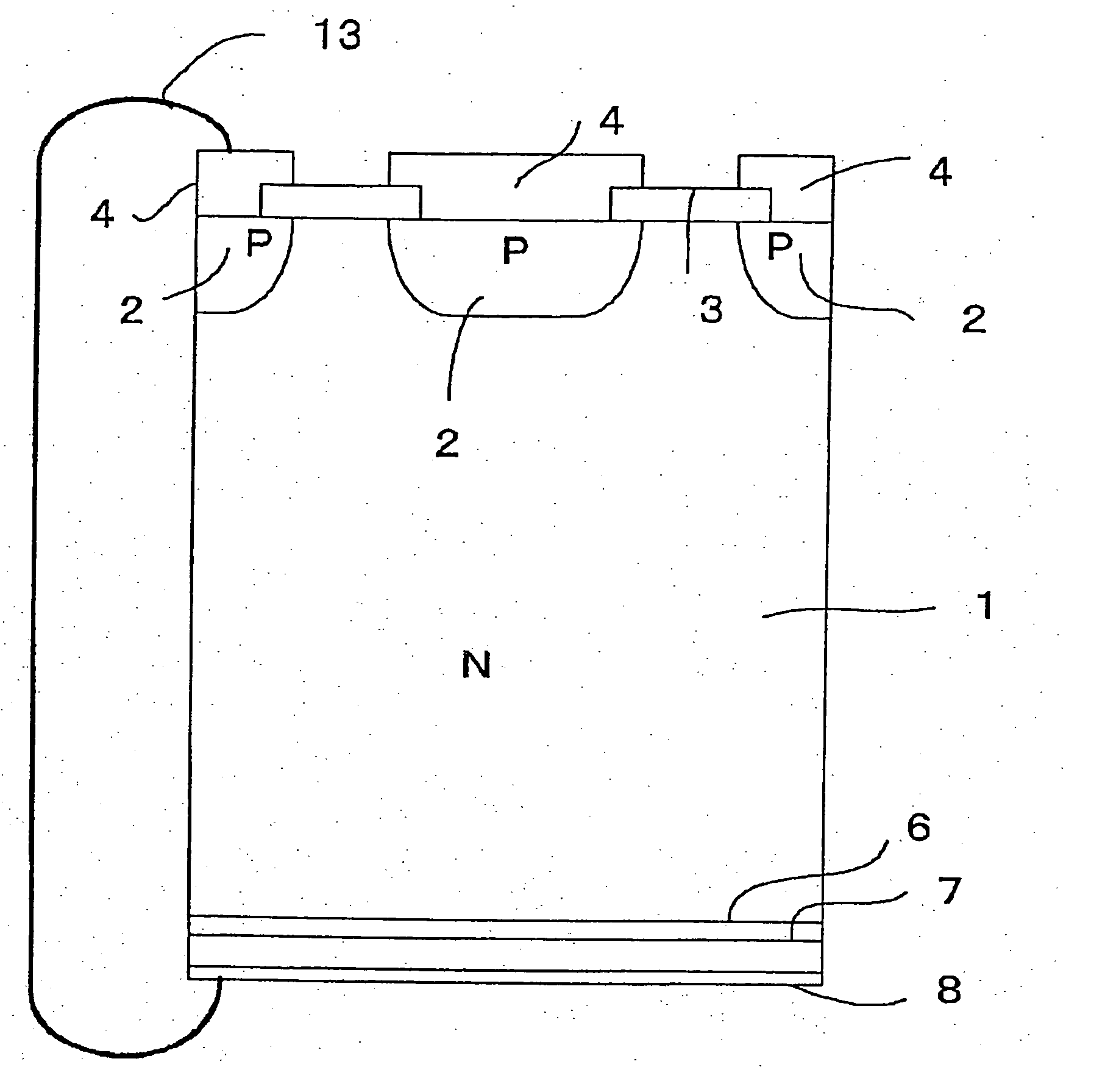
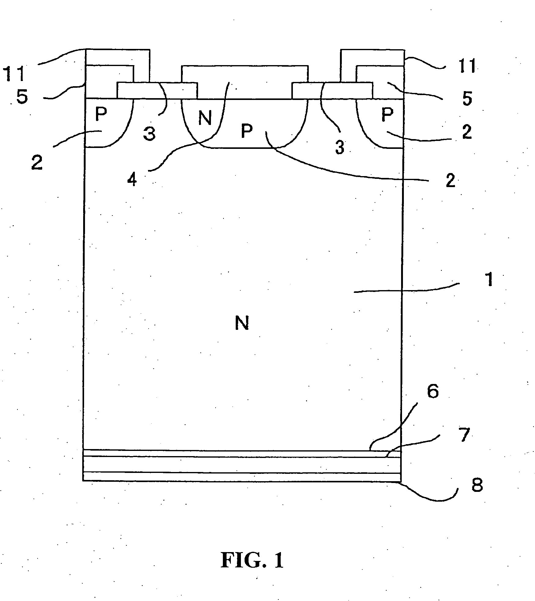
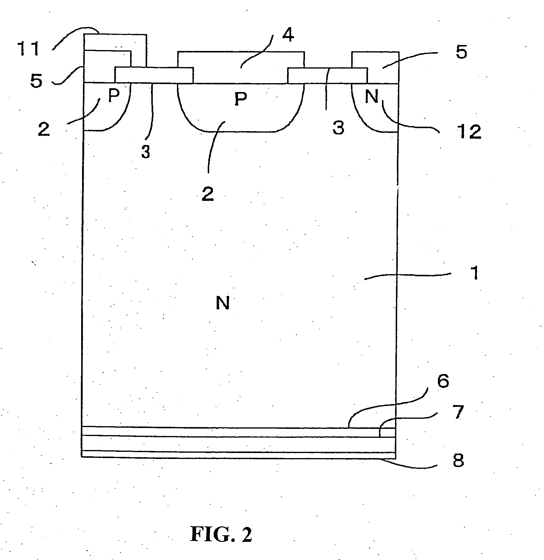
[0033]FIG. 1 is a cross sectional view of a first example according to the invention. In FIG. 1, there is shown a chip of a rectifying element with P-type diffused layers 2 selectively formed on a top surface as an anode side of N-type silicon substrate 1. On a perimeter of the top surface of the element, there is provided insulator film 3, such as an oxide film. The example is shown as one of chips after a wafer comprising a plurality of chips has been separated into individual chips along scribe lines on the wafer. A scribe line (not shown) which reached P-type diffused layer 2 was provided on the wafer at section of the wafer that would become a side face of the chip. On the scribe line, there also was provided insulator film 3, such as the oxide film or insulator film 11 of polyimide or the like. Moreover, also on the side face of the wafer, an insulator film is formed. On the surface of each of P-type diffused layers 2, there is formed aluminum electrode 4 as an anode electrode...


PUM

PropertyMeasurementUnit
thicknessaaaaaaaaaa
thicknessaaaaaaaaaa
perimeteraaaaaaaaaa

Abstract

A method of manufacturing a semiconductor device is disclosed in which a metallic deposit is stably formed on the anode side with small variation in film thickness, and plating is prevented on the cathode side without carrying out any additional processing on the cathode side. The processed anode side causes no interference in subsequent processing. Insulator films are used to cover a scribe line, as well as a field plate or an open electrode provided on a surface of a silicon substrate before Ni electroless plating of an aluminum electrode is performed to form a metallic deposit on the electrode.

Description

[0001] This application claims priority from Japanese application JP PA 2003-163401, filed on Jun. 9, 2003, the contents of which are incorporated by reference herein in their entirety. BACKGROUND OF THE INVENTION [0002] A. Field of the Invention [0003] The present invention relates to a method of manufacturing a semiconductor device in which method an electrode is formed by an electroless plating method on a semiconductor device as a rectifying element such as a diode. [0004] B. Description of the Related Art [0005] In an electric power converter device for converting direct current to alternating current or vice versa such as an inverter or a converter, a rectifying element formed of a single element semiconductor chip is used as a free wheeling diode in being connected to a power semiconductor element in inverse parallel for current free wheeling. [0006] A cross section of a unit cell structure of the diode is shown in FIG. 8. In FIG. 8, on one of surfaces of N-type silicon subst...

Claims


Application Information

Patent Timeline
21 Jul 2005
Publication
US20050158979A1
IPC
H01L21/3205; H01L21/329; H01L23/52; H01L21/288; H01L29/06; H01L29/417; H01L29/861
CPC
H01L29/417; H01L29/66136; H01L29/861; H01L2924/0002; Y10S438/928; H01L2924/00
Inventors
MOMOTA, SEIJI; MOCHIZUKI, EIJI