Method for forming interlayer insulation film

a technology of interlayer insulation and film, which is applied in the direction of semiconductor/solid-state device details, chemical vapor deposition coating, coating, etc., can solve the problems of insufficient security of transistor characteristics such as suppression of short channel effect and driving current, and the inability to use high-temperature annealing conditions, etc., to achieve short period of time and reduce damage applied to semiconductor devices.

Active Publication Date: 2005-07-21
SHARP KK
View PDF5 Cites 1 Cited by
  • Summary
  • Abstract
  • Description
  • Claims
  • Application Information

AI Technical Summary

Benefits of technology

[0024] Also, according to the method for forming the interlayer insulation film of the present invention, it is possible to perform a heat treatment for reflow at a low temperature and / or in a short period of time, and damage applied to a semiconductor device can be reduced.

Problems solved by technology

However, a demand for lowering a process temperature becomes more severe along with miniaturization of a device.
When a heat treatment of 800° C. or higher is performed in a device of 0.18 μm or less, a problem occurs in that transistor characteristics such as suppression of short channel effect and driving current cannot be sufficiently secured.
Therefore, a high temperature annealing condition cannot be used.
However, when the BPSG film is formed by a twice divided process, an interface between an upper BPSG film and a lower BPSG film is exposed in a contact forming process or an interlayer CMP process which is a subsequent process, and an abnormal shape may be produced from an etch speed difference of a wet processing due to a difference between characteristics of the upper BPSG film and that of the lower BPSG film.
However, since shrink fastening is insufficient, the film is not compact and becomes unstable.
Thus, it is difficult to form an excellent interlayer insulation film in which voids do not remain without damaging reliability of a device.

Method used


Image

  • Method for forming interlayer insulation film
  • Method for forming interlayer insulation film
  • Method for forming interlayer insulation film

Examples


example 1

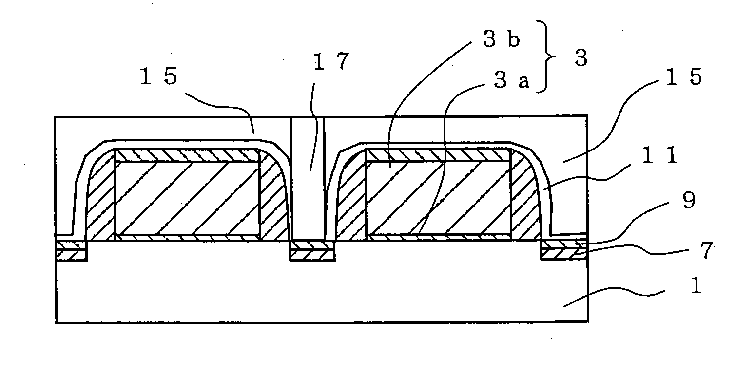
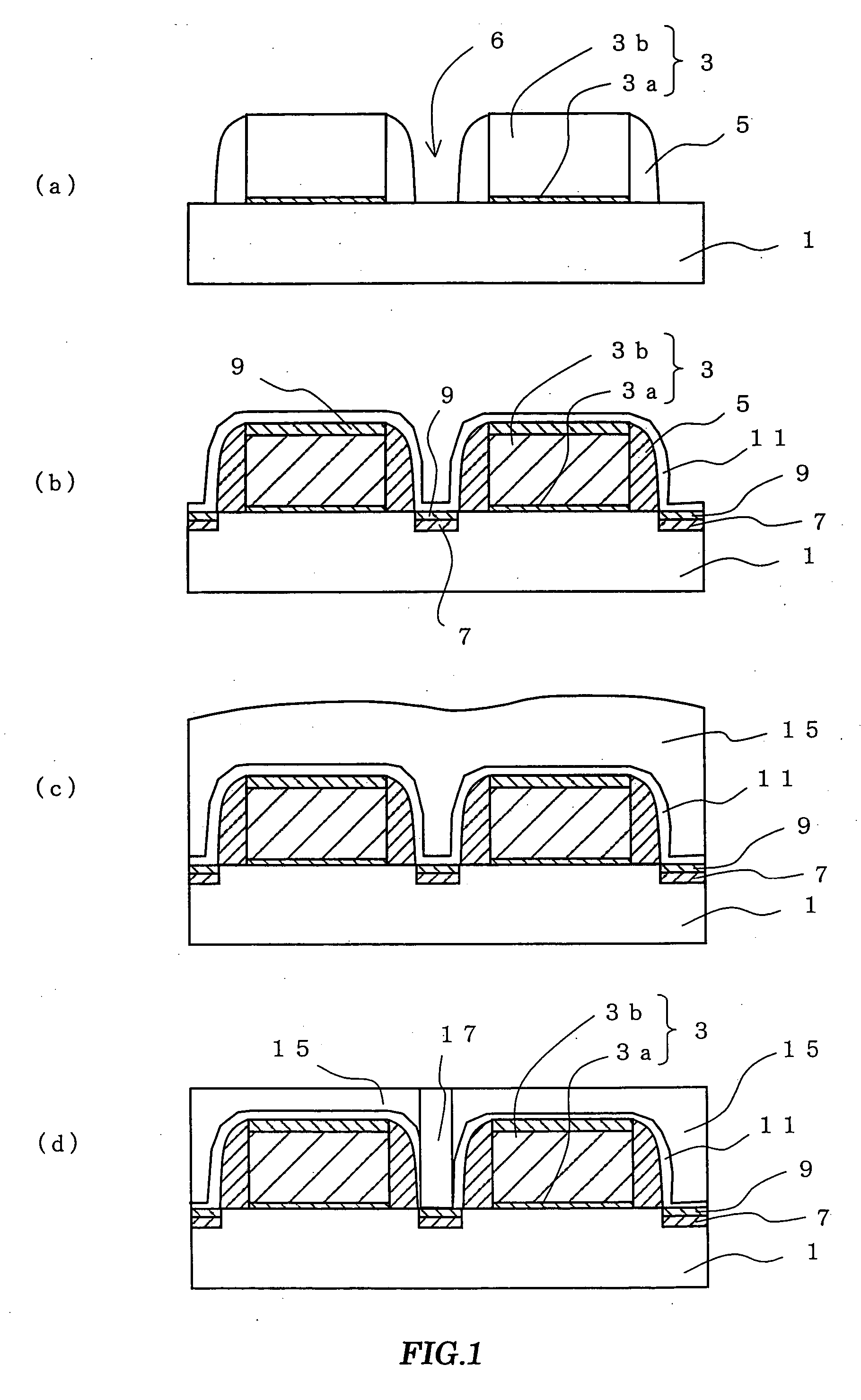
[0054]FIG. 1 is a sectional view showing a method for forming an interlayer insulation film according to Example 1 of the present invention. Hereinafter, the method for forming the interlayer insulation film according to the present Example will be described with reference to FIG. 1.

[0055] First, a polysilicon film 3b is formed through a gate insulating film 3a on a semiconductor substrate 1, and the polysilicon film 3b is then patterned to form a gate pattern 3. Next, a silicon oxide film or a silicon nitride film is formed on the entire surface of the substrate 1 so as to cover the gate pattern 3, and is etched back and removed using dry etching. Sidewalls 5 are then formed at the sidewalls of the gate pattern 3 by the residual silicon oxide film or silicon nitride film, obtaining a structure shown in FIG. 1(a). At this time, the step parts 6 are formed between the gate patterns 3.

[0056] Next, source / drain regions 7 are formed in a self-alignment manner using the gate patterns 3...

example 2

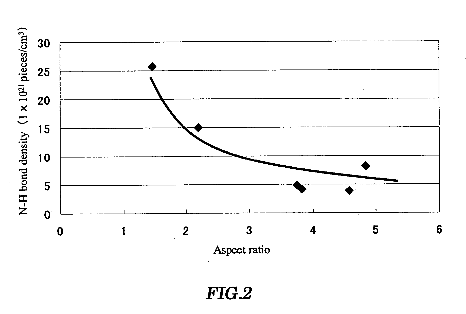
[0072]FIG. 2 shows the relationship between the aspect ratio of a step part between gates and the N—H bond density of a silicon nitride film for embedding a BPSG film in which voids do not occur in the step part between the gates. Herein, the term “aspect ratio” means a distance between the substrate and the upper surface of the gate pattern / a distance between sidewalls on the surface of the substrate. The distance between the sidewalls was determined by using a SEM.

[0073] The occurrence of voids can be suppressed in the step part by selecting film formation conditions of the silicon nitride film such that the relationship between the aspect ratio and the N—H bond density of the silicon nitride film is in a lower area of the characteristics curve inFIG. 2. The N—H bond density is measured by Fourier Transform Infrared spectroscope (FTS-40) manufactured by Bio-Rad Company.

[0074] Particularly, the graph of FIG. 2 was obtained in the following manner. First, samples in which depth of...


PUM

PropertyMeasurementUnit
temperatureaaaaaaaaaa
aspect ratioaaaaaaaaaa

Abstract

It is an object of the present invention to provide a method for forming an interlayer insulation film suppressing the occurrence of voids in the interlayer insulation film.
A method for forming an interlayer insulation film of the present invention, comprising the steps of: (1) forming an etching stopper film of a silicon nitride film on an entire surface including a step part on a semiconductor substrate having the step part with an aspect ratio of ≧3; (2) forming an interlayer insulation film of an impurity-doped silicate film on the silicon nitride film; and (3) performing reflow of the interlayer insulation film by a heat treatment, wherein the formation of the silicon nitride film is controlled such that the N—H bond density of the silicon nitride film is 1.0×10²² pieces/cm3 or less. According to the method for forming the interlayer insulation film of the present invention, the occurrence of the voids can be suppressed in the interlayer insulation film even if the aspect ratio of the step part formed on the semiconductor substrate is 3 or more. Also, the damage applied to the semiconductor device by reflow can be reduced.

Description

CROSS-REFERENCE TO RELATED APPLICATION [0001] This application is related to Japanese application No. 2004-009401 filed on Jan. 16, 2004 whose priority is claimed under 35 USC §119, the disclosure of which is incorporated by reference in its entirety. BACKGROUND OF THE INVENTION [0002] 1. Field of the Invention [0003] The invention relates to a method for forming an interlayer insulation film. [0004] 2. Description of Related Art [0005] A technique in which a step part of a high aspect ratio is embedded and flattened by an interlayer insulation film formed at low temperature has increasingly been raised in importance along with enhancement of density and integration of LSI. [0006]FIG. 3 is a process sectional view showing a conventional method for manufacturing a semiconductor device. Hereinafter, a method for manufacturing a conventional semiconductor device will be described by using FIG. 3. [0007] First, a gate insulating film 53a and a polysilicon film 53b are deposited on a sem...

Claims


Application Information

Patent Timeline
Patent Type & Authority Applications(United States)
IPC IPC(8): H01L21/28H01L21/31H01L21/314C23C16/34H01L21/316H01L21/318H01L21/768H01L23/522
CPCH01L21/3143H01L21/31625H01L21/3185H01L21/76837H01L21/76826H01L21/76828H01L21/76829H01L21/76825H01L21/02274H01L21/02164H01L21/02318H01L21/02271H01L21/0217H01L21/31
Inventor SONODA, TAKANORIMITSUMUNE, KAZUMASAABE, KENICHIROHINOUE, YUSHIDOI, TSUKASA
Owner SHARP KK
Why Eureka
Try Eureka