Semiconductor device

Active Publication Date: 2005-07-28
MITSUBISHI ELECTRIC CORP
View PDF4 Cites 48 Cited by
  • Summary
  • Abstract
  • Description
  • Claims
  • Application Information

AI Technical Summary

Benefits of technology

[0008] It is an object of the present invention to ensure an improvement in stability of withstand voltage and an increase

Problems solved by technology

At that time, if an electric field concentration (electric field peak) locally occurs in a semiconductor substrate on which the device is formed, it becomes easier to cause a breakdown in a pn junction or a breakage in an insulating film at that local portion and this

Method used


Image

  • Semiconductor device
  • Semiconductor device
  • Semiconductor device

Examples


Embodiment Construction

The First Preferred Embodiment

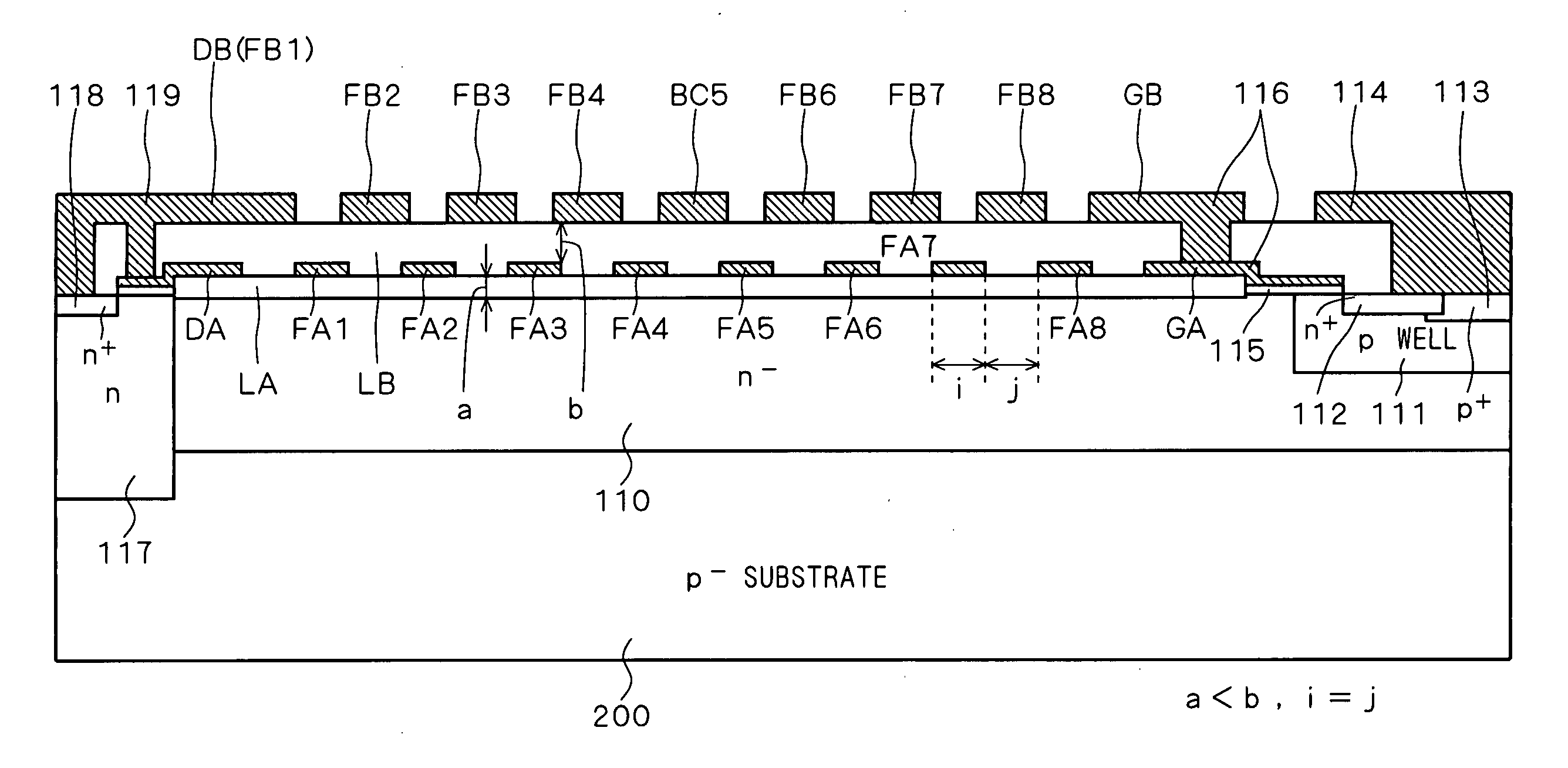
[0056]FIG. 1 is a view for explanation on an example of semiconductor device to which the present invention can be applied, showing a general-type power device and a power-device driving apparatus. In FIG. 1, n-channel type IGBTs (insulated gate bipolar transistors) 51 and 52 which are power switching devices perform switching of a high voltage HV which is a main power supply. A load is connected to a node N30 and free wheeling diodes D1 and D2 are connected to the IGBTs 51 and 52, respectively, for protecting the IGBTs 51 and 52 from a back electromotive voltage due to the load.

[0057] The power-device driving apparatus 100 for driving the IGBTs 51 and 52 operates in accordance with a high side control input HIN for controlling the high side IGBT 51 and a low side control input LIN for controlling the low side IGBT 52. The power-device driving apparatus 100 further has a high side driving unit 101 for driving the high side IGBT 51, a low side driving ...


PUM


Abstract

A p well serving as a channel region of a MOSFET is formed on one side of an n layer and an n+ drain region is formed on the other side. Above the n layer, a plurality of first floating field plates are formed with a first insulating film interposed therebetween. A plurality of second floating field plates are formed thereon with a second insulating film interposed therebetween. Assuming that the thickness of the first insulating film is “a” and the distance between the first floating field plates and the second floating field plates in a direction of thickness of the second insulating film is “b”, a relation a>b is held.

Description

BACKGROUND OF THE INVENTION [0001] 1. Field of the Invention [0002] The present invention relates to a technique to ensure improvement in stability of withstand voltage and an increase of withstand voltage in a semiconductor device, especially in a high breakdown voltage semiconductor device. [0003] 2. Description of the Background Art [0004] In order to drive two power switching devices (MOSFET, IGBT or the like) of high side and low side, for example in a half-bridge type inverter, a power-device driving apparatus having a high side (high potential island) driving circuit for driving the high side power switching device and a low side driving circuit for driving the low side power switching device. Since the high side circuit is operated with its potential in a floating state with respect to the ground potential, such a power-device driving apparatus is provided with a level shifting circuit for transmitting a driving signal to the high side driving circuit. A general-type level s...

Claims


Application Information

Patent Timeline
IPC IPC(8): H01L29/06H01L21/335H01L27/088H01L27/12H01L29/08H01L29/40H01L29/423H01L29/739H01L29/78H01L29/861
CPCH01L27/088H01L29/0878H01L29/0886H01L29/404H01L29/42368H01L2924/0002H01L29/7816H01L29/7823H01L2924/00E03C1/264E03C2201/40
Inventor HATADE, KAZUNARI
Owner MITSUBISHI ELECTRIC CORP
Why Eureka
Try Eureka