Flip-flop circuit having majority-logic circuit

a flip-flop circuit and logic circuit technology, applied in pulse manipulation, pulse technique, instruments, etc., can solve problems such as soft error, triggering malfunction across the whole chip, and corrupted data maintained in memory circuits,

Inactive Publication Date: 2005-07-28
FUJITSU LTD
View PDF9 Cites 21 Cited by
  • Summary
  • Abstract
  • Description
  • Claims
  • Application Information

AI Technical Summary

Benefits of technology

[0028] The majority-logic circuit makes it possible, even when a soft error takes place, to output corr

Problems solved by technology

There is a phenomenon, known as a soft error, such that data maintained in a memory circuit, etc., are corrupted.
On the other hand, as for some data such as parameter values of a timing-adjusting circuit, there is a high likelihood that an occurrence of the soft error as described above triggers malfunctioning across the whole chip.
More specifically, data set during the period of an initializing operation of a system, etc., are not rewritten after the initializing is terminated for starting an actual operation, so that the corrupted data continue to be maintained, often resulting in a malfunction.
However, a problem exists such that, for using the conve

Method used


Image

  • Flip-flop circuit having majority-logic circuit
  • Flip-flop circuit having majority-logic circuit
  • Flip-flop circuit having majority-logic circuit

Examples


first embodiment

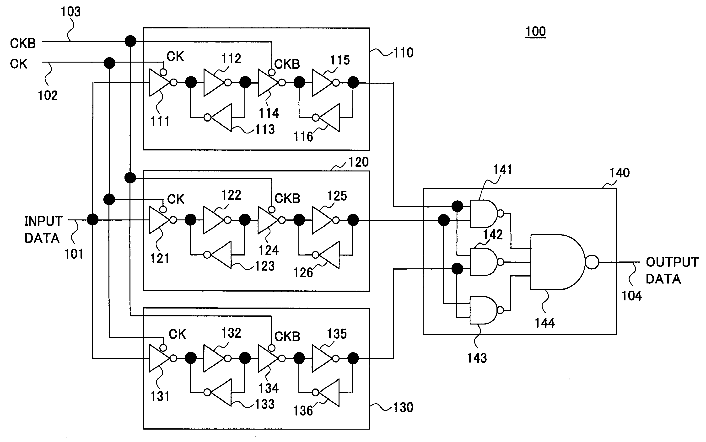
[0068] Moreover, two additional master latches can be removed from the first embodiment according to the present embodiment so as to make it possible to provide a flip-flop circuit with the circuit size reduced further from the related art as illustrated in FIG. 1. A feedback transistor has an irregular circuit layout and a coverage area within a LSI chip that is larger than a typical transistor, so that there is a great advantage in reducing the area.

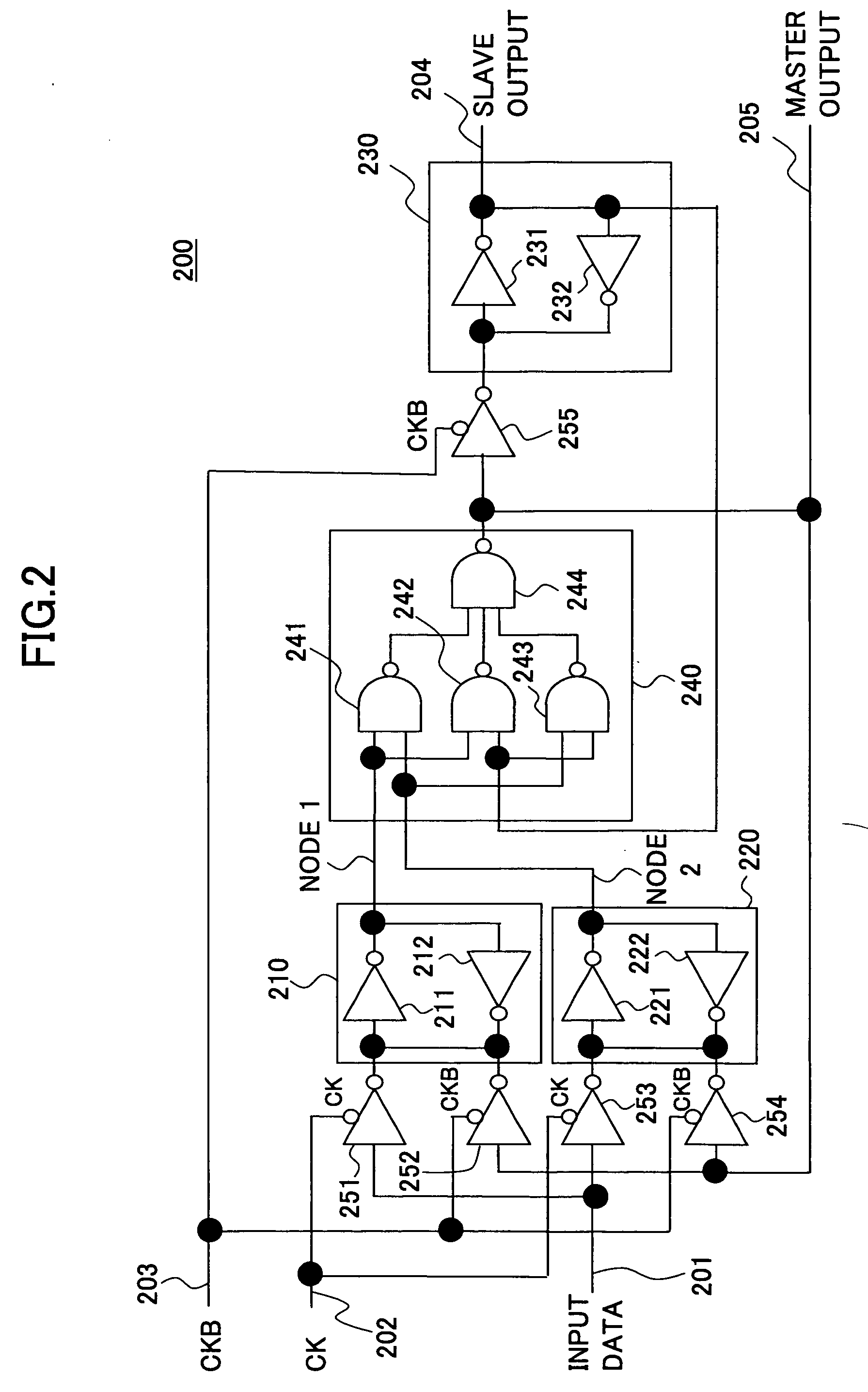
[0069] Next, a comparison between the operation of the flip-flop circuit 200 of the first embodiment or the flip-flop circuit 300 of the second embodiment of the present invention and the operation of a conventional one flip-flop is described. FIG. 6 is a diagram illustrating the comparison of the operation of the flip-flop circuit of the first embodiment or the second embodiment of the present invention and the operation of, for example, the conventional one flip-flop such as the flip-flop 110 in FIG. 1 when a soft error does not take...

third embodiment

[0112]FIG. 10 is a diagram for illustrating the present invention for use in a circuit for setting a signal for controlling a memory. FIG. 10 is an embodiment for storing a 3-bit parameter value for adjusting a sense-amplifier starting-timing. The 3-bit parameter value for adjusting the sense-amplifier starting-timing stored in flip-flops 1002, 1003, and 1004 of the embodiment of the present invention is input via signal lines 1005, 1006, and 1007. Using the parameter value, an error at the time of designing the sense amplifier or a dispersion in manufacturing may be absorbed. Moreover, if the RAM can operate at high speed, the starting timing of the sense amplifier can be set ahead to achieve an improvement in the performance. On the other hand, when the RAM operation is unstable, the starting timing of the sense amplifier can be delayed to maintain an operating margin.

[0113] While a flip-flop circuit of the embodiments of the present invention is applied to the flip-flop circuit f...


PUM


Abstract

A flip-flop circuit having a majority-logic circuit is disclosed. The circuit further includes multiple master latches for writing in corresponding input signals, and one slave latch having an input connected to an output of the majority-logic circuit and an output connected to the inputs of the majority-logic circuit. The majority logic-circuit has multiple inputs connected to respective outputs of the master latches. During the period in which the master latches do not write in the corresponding input signals, an output signal of the majority-logic circuit is supplied to respective inputs of the master latches.

Description

CROSS-REFERENCE TO RELATED APPLICATION [0001] This application is a U.S. continuation application filed under 35 USC 111(a) claiming benefit under 35 USC 120 and 365(c) of PCT application JP03 / 06356, filed May 21, 2003, which is hereby incorporated by reference.BACKGROUND OF THE INVENTION [0002] 1. Field of the Invention [0003] The present invention generally relates to a technology for a flip-flop circuit, and particularly relates to a flip-flop circuit having a majority-logic circuit for making it possible, even when a soft error takes place, to output correct storage contents and to recover from the soft error so as to maintain the correct storage contents. [0004] 2. Description of the Related Art [0005] There is a phenomenon, known as a soft error, such that data maintained in a memory circuit, etc., are corrupted. The soft error is a phenomenon such that alpha rays generated from LSI-chip materials as well as secondary cosmic-ray neutrons causing electric charges to be generate...

Claims


Application Information

Patent Timeline
IPC IPC(8): G11C7/06G11C7/10G11C11/412H03K3/037H03K5/135
CPCG11C7/06G11C7/1045H03K5/135G11C11/4125H03K3/0375G11C11/41
Inventor SATSUKAWA, YOSHIHIKO
Owner FUJITSU LTD
Why Eureka
Try Eureka