Display element and display device

a display element and display device technology, applied in liquid crystal compositions, instruments, chemistry apparatus and processes, etc., can solve the problems of slow response of liquid crystal display elements using tn mode, large hindrances of tn mode, narrow viewing angle, etc., to reduce the effect of coloring phenomenon, reduce the driving voltage, and improve contras

Active Publication Date: 2005-07-28
MERCK PATENT GMBH
View PDF4 Cites 24 Cited by
  • Summary
  • Abstract
  • Description
  • Claims
  • Application Information

AI Technical Summary

Benefits of technology

[0021] An object of the present invention is to attain a low driving voltage as low as a practical level, improved contrast, and alleviation in coloring

Problems solved by technology

The liquid crystal display elements using the TN mode have disadvantages of slow response, narrow viewing angle, and the other drawbacks.
Those disadvantages are large hindrances for the TN mode to take over CRT (Cathode Ray Tube).
Moreover, the display modes in which the FLC or AFLC is used, are advantageous in their fast response and wide viewing angles, but significantly poor in anti-shock property and temperature characteristics.
Therefore, the display modes in which the FLC or AFLC is used have not been widely used.
However, in principle, the polymer dispersion type liquid crystal display mode cannot control the viewing angle by using a phase plate (retardation film).
Further, the polymer dispersion type liquid crystal display mode has a problem in terms of its response property.
Thus, the polymer dispersion type liquid crystal display mode is generally not as advantageous as the TN mode.
On this account, all these display methods have viewing angle limits.
The display modes in which the FLC and the AFLC are used[ ] are advantageous in terms of response speed and viewing angle, but have a problem in that their alignment can be irreversibly destroyed by an external force.
A significant practical problem to be overcome for utilizing the Kerr effect in display elements is that utilization of the Kerr effect requires a larger driving voltage compared with convention

Method used


Image

  • Display element and display device
  • Display element and display device
  • Display element and display device

Examples


Embodiment Construction

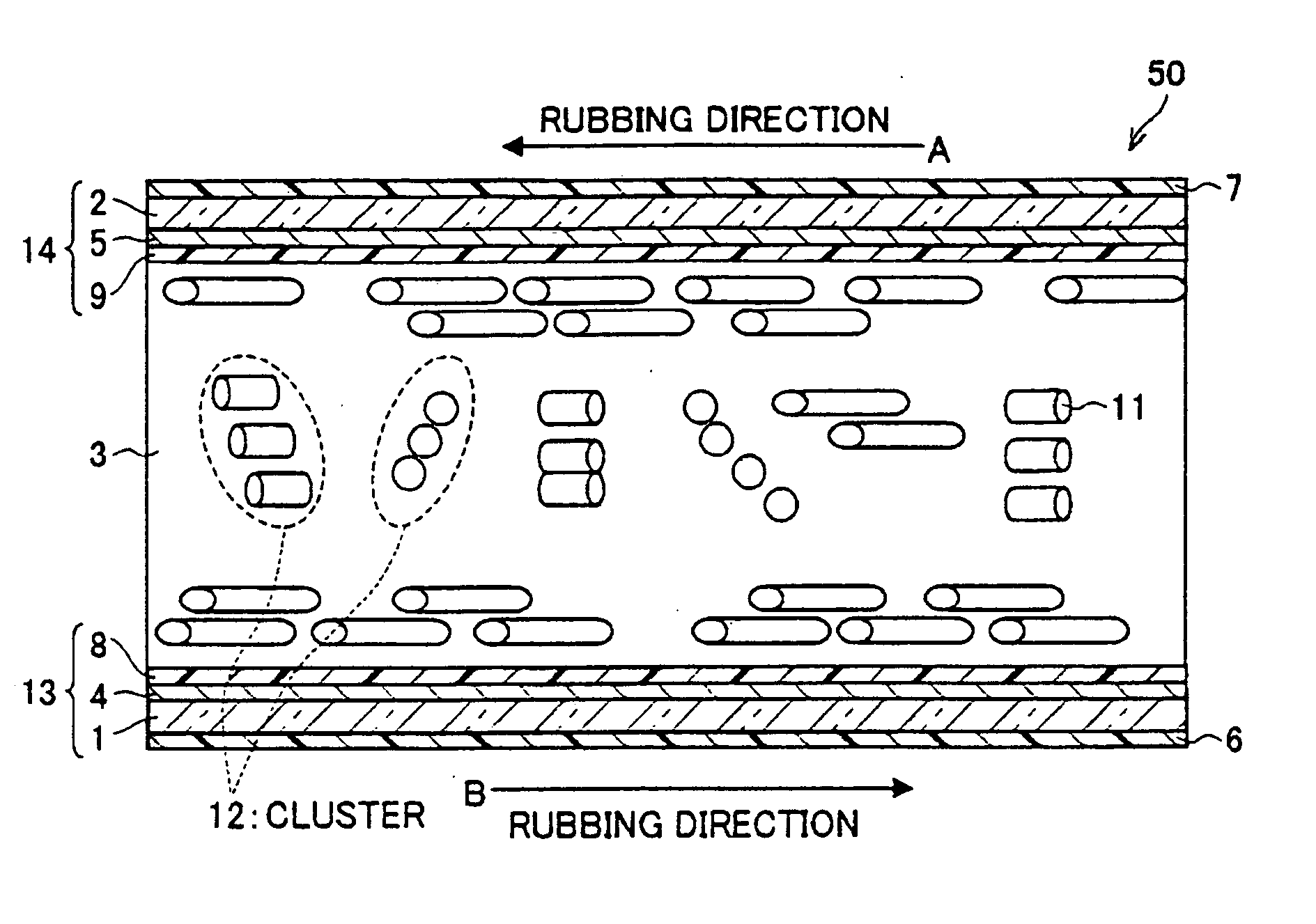
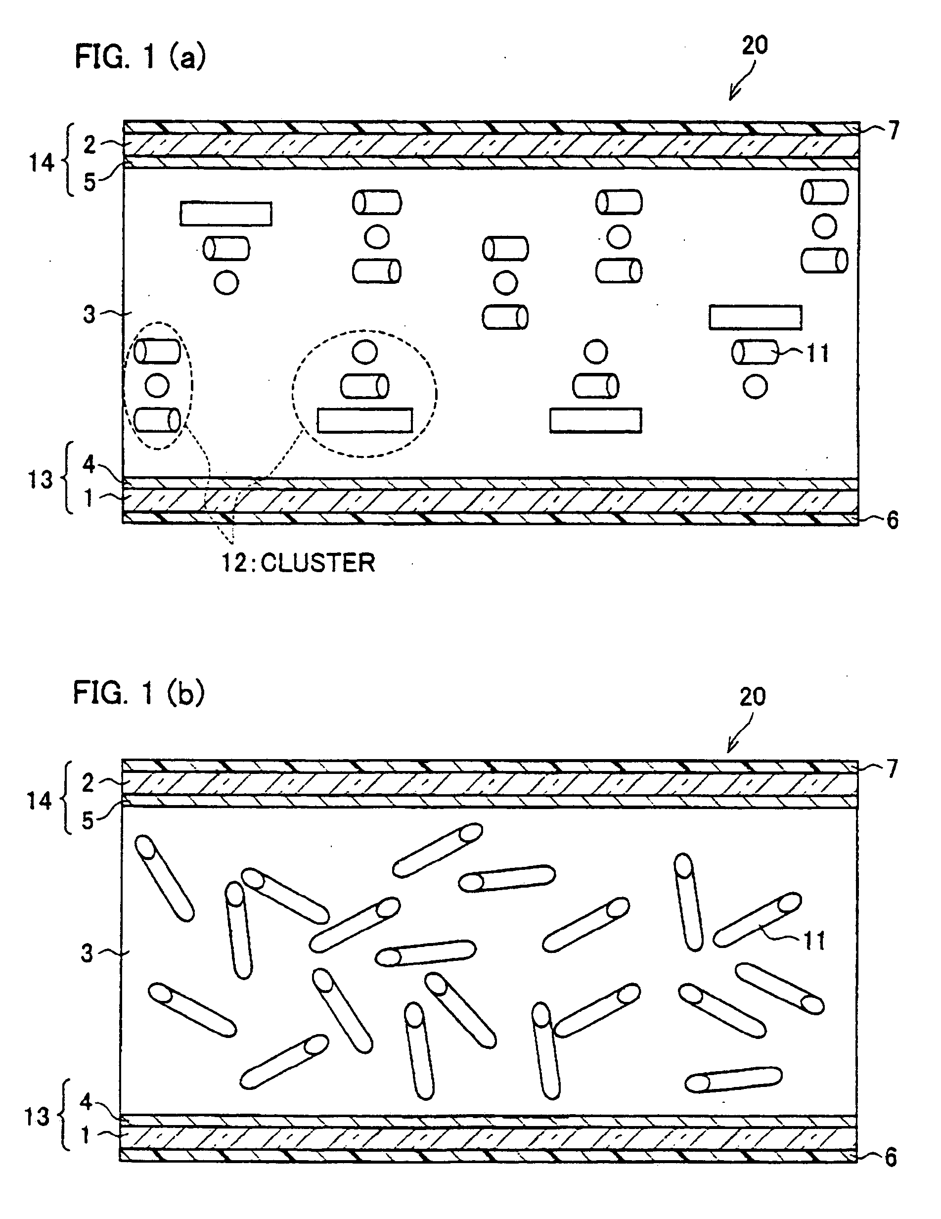
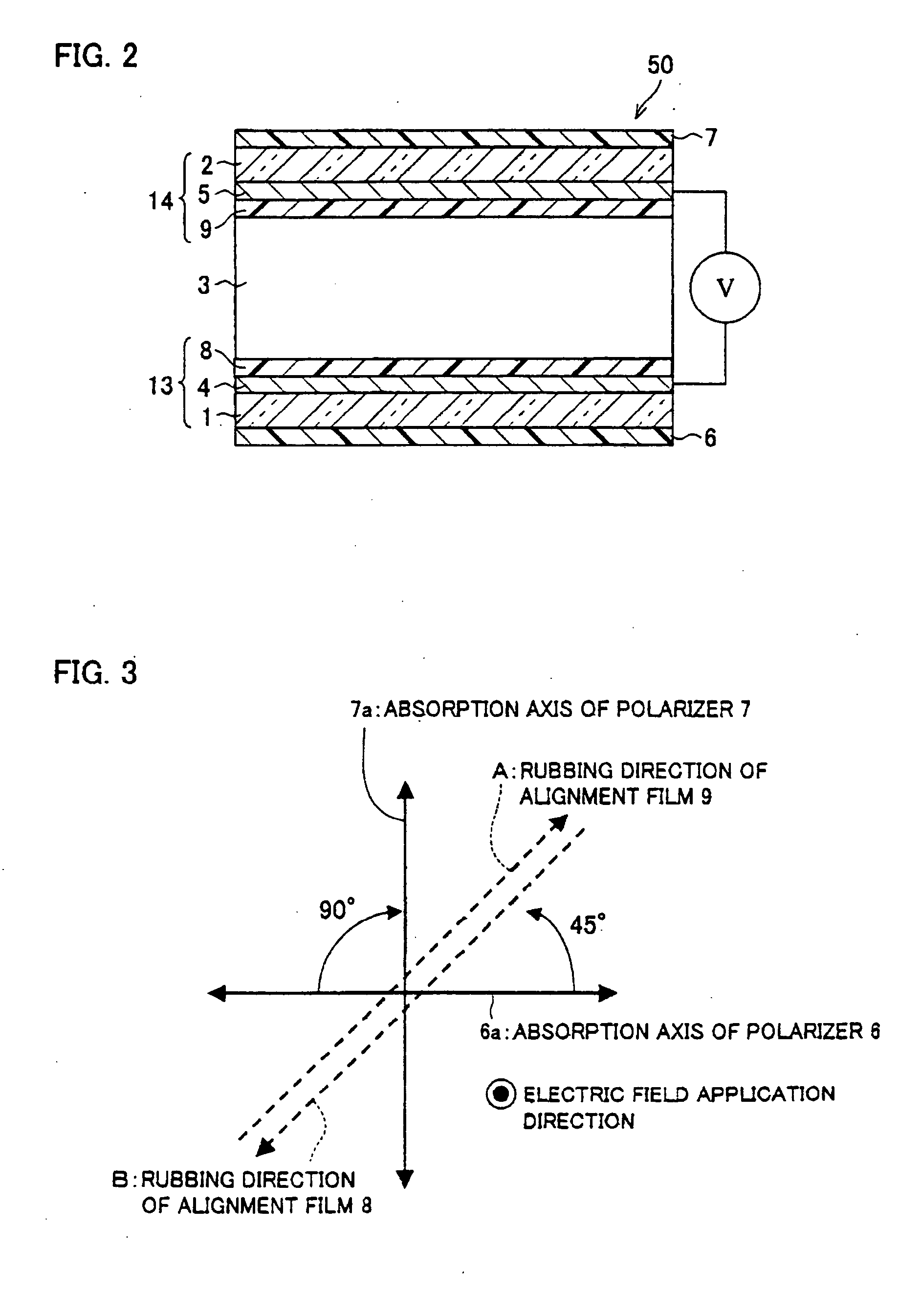
[0067] A non-limiting, example embodiment is described with reference to FIGS. 1 to 17. FIGS. 1(a) and 1(b) are schematic cross sectional views schematically illustrating an arrangement of a display element according to an example implementation of the present embodiment. FIG. 1(a) illustrates the display element when an electric field is applied between the substrates and FIG. 1(b) illustrates the display element when no electric field is applied. Moreover, FIG. 5 schematically illustrates an arrangement of various parts of a display device in which the display element according to the present embodiment is used. FIG. 6 schematically illustrates an arrangement of a periphery of the display element used in the display device illustrated in FIG. 5.

[0068] The display element according to the present embodiment can be used in a display device. A driving circuit, signal lines (e.g., data signal lines), scanning lines (e.g., scanning signal lines), switching elements or the like are als...


PUM


Abstract

An electrode is provided on one surface of each of a pair of substrates. On the other surface of each of the substrates, a polarizer is provided. The substrates are assembled together so that their surfaces on which the electrodes are formed face each other. Then, a medium is introduced between the substrates, to form a dielectric material layer. The medium is prepared by mixing a chiral agent in a negative type liquid crystalline compound.

Description

[0001] This Nonprovisional application claims priority under 35 U.S.C. § 119(a) on Patent Applications Nos. 2004 / 8471, 2004 / 253607, and 2005 / 6865 filed in Japan respectively on Jan. 15, 2004, Aug. 31, 2004 and on Jan. 13, 2005, the entire contents of which are hereby incorporated by reference.FIELD OF THE INVENTION [0002] The present invention relates to a display element and display device having excellent display properties, including, e.g., high-speed response and wide-viewing angle. BACKGROUND OF THE INVENTION [0003] Liquid crystal display elements are advantaged over other display elements in terms of its thin thickness, light weight, and low power consumption. The liquid crystal display elements are widely used in image display apparatuses such as televisions, video cassette recorders, and the like, and OA (Office Automation) apparatuses such as monitors, word processors, personal computers, and the like. [0004] Conventionally known liquid crystal display methods of the liquid...

Claims


Application Information

Patent Timeline
IPC IPC(8): G02F1/1337C09K19/18C09K19/20C09K19/58G02F1/1343G02F1/1368G02F1/139
CPCC09K19/18C09K19/2007C09K19/586G02F1/1396G02F1/134363G02F1/1368G02F1/1393G02F1/133784G02F1/1337
Inventor MIYACHI, KOICHIINOUE, IICHIROSHIBAHARA, SEIJIISHIHARA, SHOICHI
Owner MERCK PATENT GMBH
Why Eureka
Try Eureka