Display device, method for manufacturing thereof, and television device

a technology for a display device and a manufacturing method, which is applied in the field of display devices, can solve the problems of increasing the manufacturing cost eventually, the inability of the technique to drastically reduce the number of photolithography steps, and the inability to expose a large-size substrate with 1 m on a side at once, so as to prevent the oxidation of the gate electrode layer, eliminate waste of materials, and improve the effect of controllability

Inactive Publication Date: 2005-07-28
SEMICON ENERGY LAB CO LTD
View PDF3 Cites 90 Cited by
  • Summary
  • Abstract
  • Description
  • Claims
  • Application Information

AI Technical Summary

Benefits of technology

[0008] It is an object of the present invention to provide a method for reducing the number of photolithography steps in steps for manufacturing a TFT, an electronic circuit using the TFT, and a display device using the TFT so as to simplify the manufacturing steps. Accordingly, a large-size substrate with 1 m or more on a side can be processed at lower cost with good yield.
[0009] It is another object of the invention to provide a method for forming a pattern of a wiring etc. with respect to a display device in a predetermined shape with good controllability.
[0010] According to the invention, a pattern having a predetermined width can be formed with excellent controllability, regardless of the size of a discharge port through which a liquid droplet is discharged.
[0032] The gate insulating layer is formed by sequentially laminating a first silicon nitride film, a silicon oxide film, and a second silicon nitride film, and therefore, oxidation of the gate electrode layer can be prevented. A favorable interface between the gate insulating layer and the semiconductor layer that is formed on the gate insulating layer can be obtained.
[0033] According to the invention, a predetermined pattern can be formed with good controllability while eliminating wasting materials, thereby reducing cost. Therefore, a high-performance, high reliable display device can be manufactured with excellent yield.

Problems solved by technology

Increasing the number of steps for photolithography increases the manufacturing cost eventually.
Therefore, the technique cannot drastically contribute to reducing the number of steps for photolithography.
Therefore, it is technically impossible to expose a large-size substrate with 1 m on a side at once, in principle.

Method used


Image

  • Display device, method for manufacturing thereof, and television device
  • Display device, method for manufacturing thereof, and television device
  • Display device, method for manufacturing thereof, and television device

Examples


embodiment mode 2

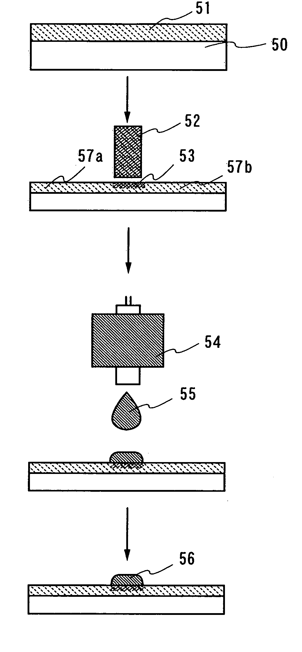
[0124] Another embodiment mode of the invention will be described with reference to FIGS. 2A to 2C, FIGS. 3A to 3C, FIGS. 4A to 4C, FIGS. 5A to 5C, FIGS. 6A to 6C, FIGS. 7A to 7C, and FIGS. 8A and 8B. Concretely, a method of manufacturing a display device (a light emitting display device) according to the invention will be described below.

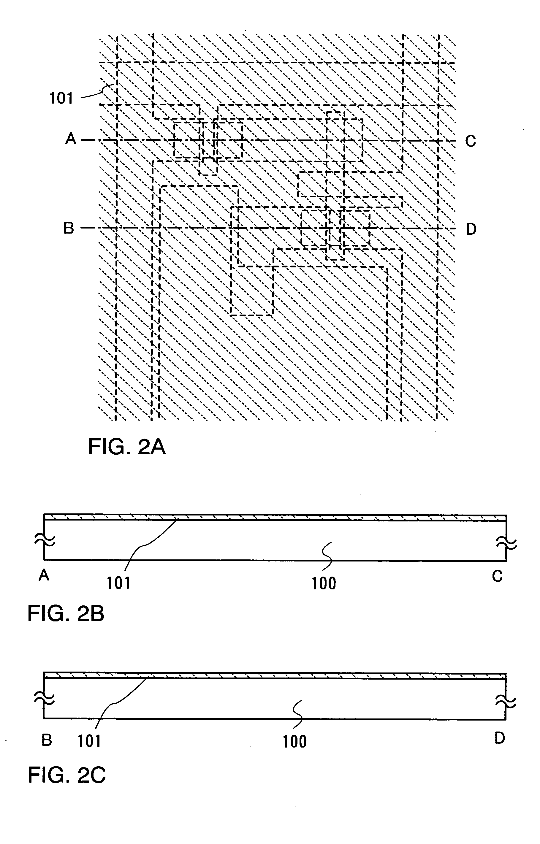
[0125] Firstly, a method of manufacturing a display device (a light emitting display device) having a channel-etched type thin film transistor according to the invention will be described. FIGS. 2A, 3A, 4A, 5A, 6A, and 7A are top views showing pixel portions of display devices, respectively. FIGS. 2B, 4B, 5B, 6B, and 7B are cross sectional views along lines A-C of the respective top views, whereas FIGS. 2C, 3C, 4C, 5C, 6C, and 7C are cross sectional views along lines B-D thereof.

[0126] A base film 101 is formed on a substrate 100 as a base pretreatment. As the substrate 100, a glass substrate such as a barium borosilicate glass and an alumino bor...

embodiment mode 3

[0194] Another embodiment mode of the invention will be described with reference to FIGS. 9A to 9C, FIGS. 10A to 10C, FIGS. 11A to 11C, and FIGS. 12A to 12C. The present embodiment mode shows an example in which a pretreatment for forming a pattern by the droplet discharging method is different of that in Embodiment Mode 1. FIGS. 9A, 10A, 11A, and 12A are top views of pixel portions for display devices. FIGS. 9B, 10B, 11B, and 12B are cross sectional views taken along each line A-C, while FIGS. 9C, 10C, 11C, and 12C are cross sectional views taken along each line B-D in the respective top views.

[0195] A base film 201 is formed over a substrate 200 as a base pretreatment. The base film 201 is made from a photosensitive material that is photoactivated with laser beam irradiation such that the base film formed in a subject region on which patterns will be formed is removed.

[0196] In FIGS. 9A to 9C, the thickness of a base film 201 is set to be equal to or thicker than the thickness o...

embodiment mode 4

[0202] Another embodiment mode of the invention will be described referring to FIG. 14, FIGS. 15A to 15D, and FIGS. 16A to 16C. The embodiment mode shows an example wherein a top-gate (staggered type) thin film transistor is used as substitute for the bottom gate (reverse stagger type) thin film transistor in Embodiment Mode 2, and therefore, identical portions or portions having similar functions to those in Embodiment Mode 2 will not be described. FIGS. 15A to 15D and FIGS. 16A to 16C are cross sectional views taken along a line B-D in FIG. 14.

[0203] A base film 301 is formed over a substrate 300 as a base pretreatment. Laser beam is selectively irradiated only to subject regions on which source or drain electrode layers 311, 312, 313, and 314 will be formed. The properties of the regions irradiated with the laser beam (i.e., base films 302a, 302b, and 302c) are changed to exhibit higher lyophilic (i.e., lower lyophobic) properties with respect to droplets made from a composition...


PUM

PropertyMeasurementUnit
widthaaaaaaaaaa
sizeaaaaaaaaaa
sizeaaaaaaaaaa

Abstract

The invention provides a display device and a method for manufacturing thereof by increasing a material efficiently as well as simplifying steps. Also, the invention provides a technique for forming a pattern such as a wiring, that is used for forming a display device, to have a predetermined shape with an excellent controllability. The method for manufacturing a display device includes the steps of: forming a lyophobic region; selectively irradiating laser beam in the lyophobic region to form a lyophilic region; selectively discharging a composition, that contains a conductive material, in the lyophilic region to form a gate electrode layer; forming a gate insulating layer and a semiconductor layer over the gate electrode layer; discharging a composition containing a conductive material over the semiconductor layer to form a source electrode layer and a drain electrode layer; and forming a pixel electrode layer on the source or drain electrode layer.

Description

BACKGROUND OF THE INVENTION [0001] 1. Field of the Invention [0002] The present invention relates to a display device and a method for manufacturing the same. The invention further relates to a television device utilizing the display device and the method for manufacturing thereof. [0003] 2. Description of the Related Art [0004] A thin film transistor (hereinafter, referred to as a TFT) and an electronic circuit using the TFT have been formed as follows: various kinds of thin films such as as semiconductor, an insulator, and a conductor are laminated over a substrate, and the thin films are processed into a predetermined pattern by photolithography. Photolithography is a technique for transferring a pattern such as a circuit, which is formed of a light-shielding material over a flat transparent plate that is referred to as a photomask, over a substrate by utilizing light. The technique has been widely used in a step of manufacturing a semiconductor integrated circuit, and the like. ...

Claims


Application Information

Patent Timeline
Patent Type & Authority Applications(United States)
IPC IPC(8): C25B11/00G09G3/20G09G3/32H01L21/77H01L27/32H01L51/52H05B33/10H05B33/22H05B44/00
CPCG09G3/3208G09G3/3225G09G2300/0842G09G2300/0861G09G2310/0251H01L27/1292H01L51/0022H01L51/055H01L51/529H01L27/1285H01L27/3244H10K59/12H10K71/611H10K10/481H10K50/87
Inventor YAMAZAKI, SHUNPEINAKAMURA, OSAMUMAEKAWA, SHINJIFUJII, GENISA, TOSHIYUKI
Owner SEMICON ENERGY LAB CO LTD
Why Eureka
Try Eureka