Method for manufacturing a semiconductor device

Inactive Publication Date: 2005-07-28
RAMBUS INC
View PDF12 Cites 7 Cited by
  • Summary
  • Abstract
  • Description
  • Claims
  • Application Information

AI Technical Summary

Benefits of technology

[0012] In view of the above, it is an object of the present invention to provide a method for manufacturing a semiconductor device, such as DRAM and SRAM devices, by performing a treatment on the vacancy type defects

Problems solved by technology

Consequently, the junction electric field between the channel layer and the source/drain diffused region becomes large, causing an increase in the junction leakage current, which lowers the data retention capability of memor

Method used


Image

  • Method for manufacturing a semiconductor device
  • Method for manufacturing a semiconductor device
  • Method for manufacturing a semiconductor device

Examples


Embodiment Construction

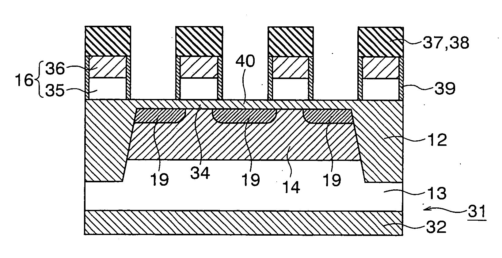
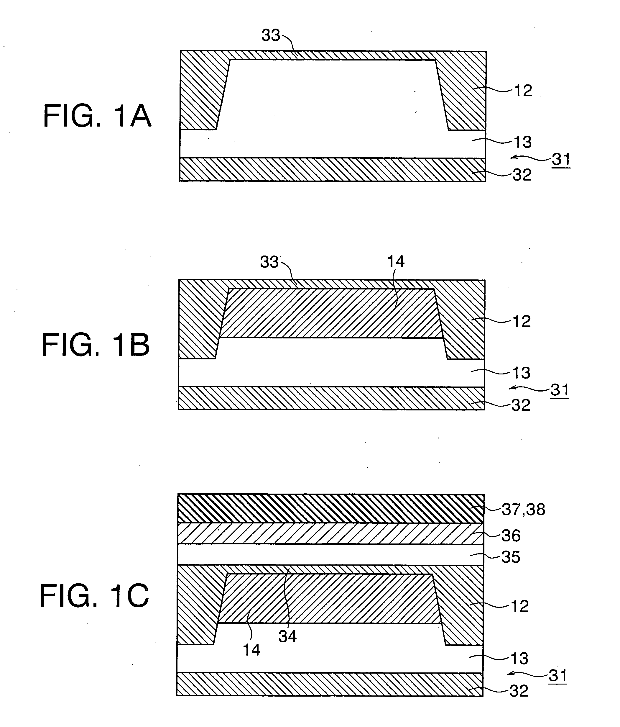
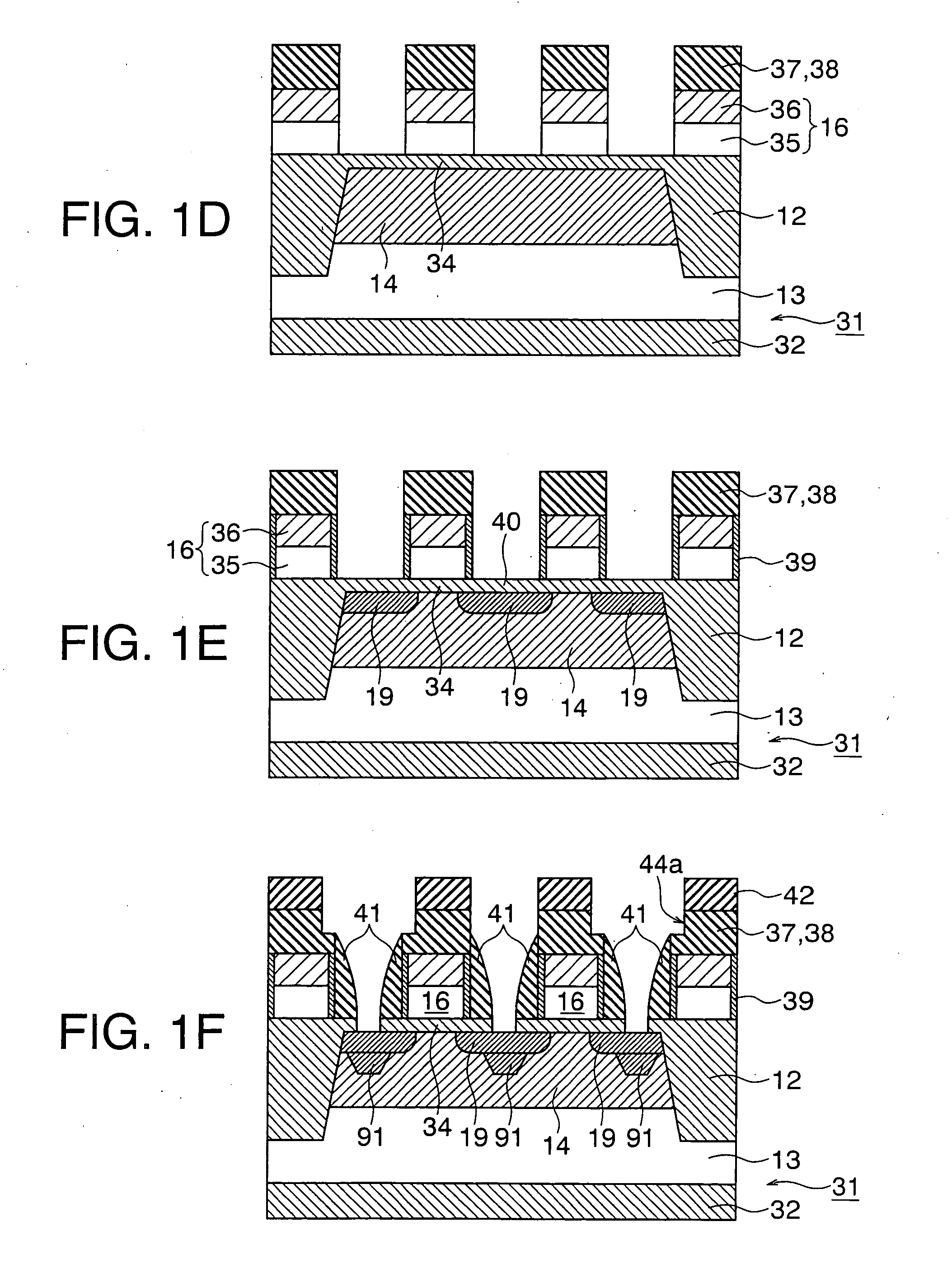
[0028] The present inventors have had the following discussions prior to the present invention. In general cases, vacancies and interstitial silicon are formed in a silicon substrate by dopant implantation for forming source / drain diffused regions. However, the interstitial silicon is diffused quickly by a heat treatment performed after the dopant implantation. Therefore, vacancies become excessive in the source / drain diffused regions. These vacancies are concentrated on the end portion of a gate electrode within the source / drain diffused regions and stay therein because this part is a stress riser where the stress is concentrated. The present inventors hence reached an assumption that, if the heat treatment is carried out in an oxidizing ambient, the interstitial silicon atoms are generated at the interface between a growing oxide film and the silicon substrate on the substrate surface. The interstitial silicon atoms can alleviate the situation of the excessive existence of vacanci...


PUM


Abstract

A method for forming a semiconductor memory device includes the steps of: implanting a dopant in a semiconductor substrate; heat treating the semiconductor substrate in an oxidizing ambient to diffuse the dopant for forming diffused regions in the semiconductor substrate; and forming memory cells each including a MOS transistor having the diffused regions as source/drain regions.

Description

BACKGROUND OF THE INVENTION [0001] 1. Field of the Invention [0002] The present invention relates to a method for manufacturing a semiconductor device, and more specifically, to a method for manufacturing a semiconductor device, which is suited to manufacture of memory cells in DRAM devices, SRAM devices, and the like for use in mobile information terminals such as cellular phones. [0003] 2. Description of Related Art [0004] Memory cells in DRAMs or SRAMs used in mobile information terminals especially require MOS transistors that cause a small junction leakage current. FIG. 9 shows a structure of a semiconductor device described in Patent Publication JP-A-2003-17586, as an example of a conventional semiconductor device. [0005] In the semiconductor device 51, a plurality of MOS transistors arranged in the form of pairs of transistors which share a bit line 11 are formed on a semiconductor substrate 31, as shown in the figure. The semiconductor substrate 31 has shallow-trench isolati...

Claims


Application Information

Patent Timeline
IPC IPC(8): H01L21/265H01L21/324H01L21/336H01L21/8242H01L27/108H01L29/78
CPCH01L21/2652H01L21/324H01L29/6659H01L27/10873H01L27/10814H10B12/315H10B12/05H01L21/18
Inventor OKONOGI, KENSUKEOYU, KIYONORI
Owner RAMBUS INC
Why Eureka
Try Eureka