Vapor deposition mask and organic EL display device manufacturing method

a technology of organic el and manufacturing method, which is applied in the direction of vacuum evaporation coating, photomechanical equipment, instruments, etc., can solve the problems of increased substrate structure manufacturing cost, scratching or peeling of organic el film formed in the previous process, and damage, etc., to achieve high pattern accuracy

Inactive Publication Date: 2005-08-04
FUJIFILM HLDG CORP +1
View PDF11 Cites 124 Cited by
  • Summary
  • Abstract
  • Description
  • Claims
  • Application Information

AI Technical Summary

Benefits of technology

[0016] Accordingly, it is an object of the present invention to provide a vapor deposition mask structure with high pattern accuracy particularly at mask openings without having to change the substrate structure.

Problems solved by technology

In this case, the deposition surface positioned on a substrate repeatedly comes into contact with the metal mask, and a metal mask to be used in a next process comes into contact with a deposition surface of a previous process so that the organic EL film formed in the previous process may be scratched or peeled, and damaged.
However, in the case of providing protruding structures as described above, a process is required for forming such protruding structure on the substrate, which may lead to an increase in manufacturing costs of the substrate structure.
However, in this example, the R, G, and B color pixels are respectively arranged into columns to form a matrix pixel structure and the mask openings are simply arranged into a striped pattern so that maintaining the mask structure becomes difficult due to distortions and deviations and the color layers of the pixels may not be accurately created.

Method used


Image

  • Vapor deposition mask and organic EL display device manufacturing method
  • Vapor deposition mask and organic EL display device manufacturing method
  • Vapor deposition mask and organic EL display device manufacturing method

Examples


embodiment 1

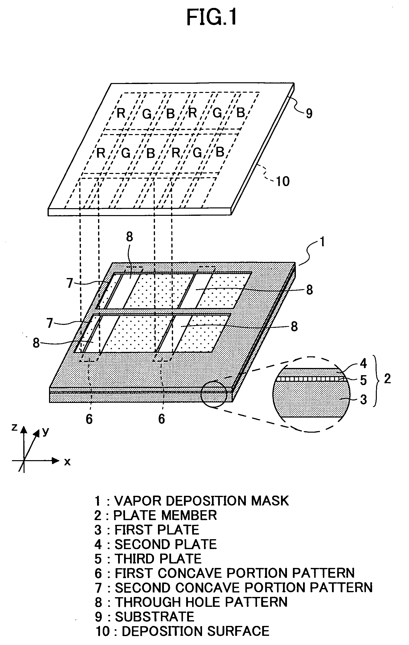
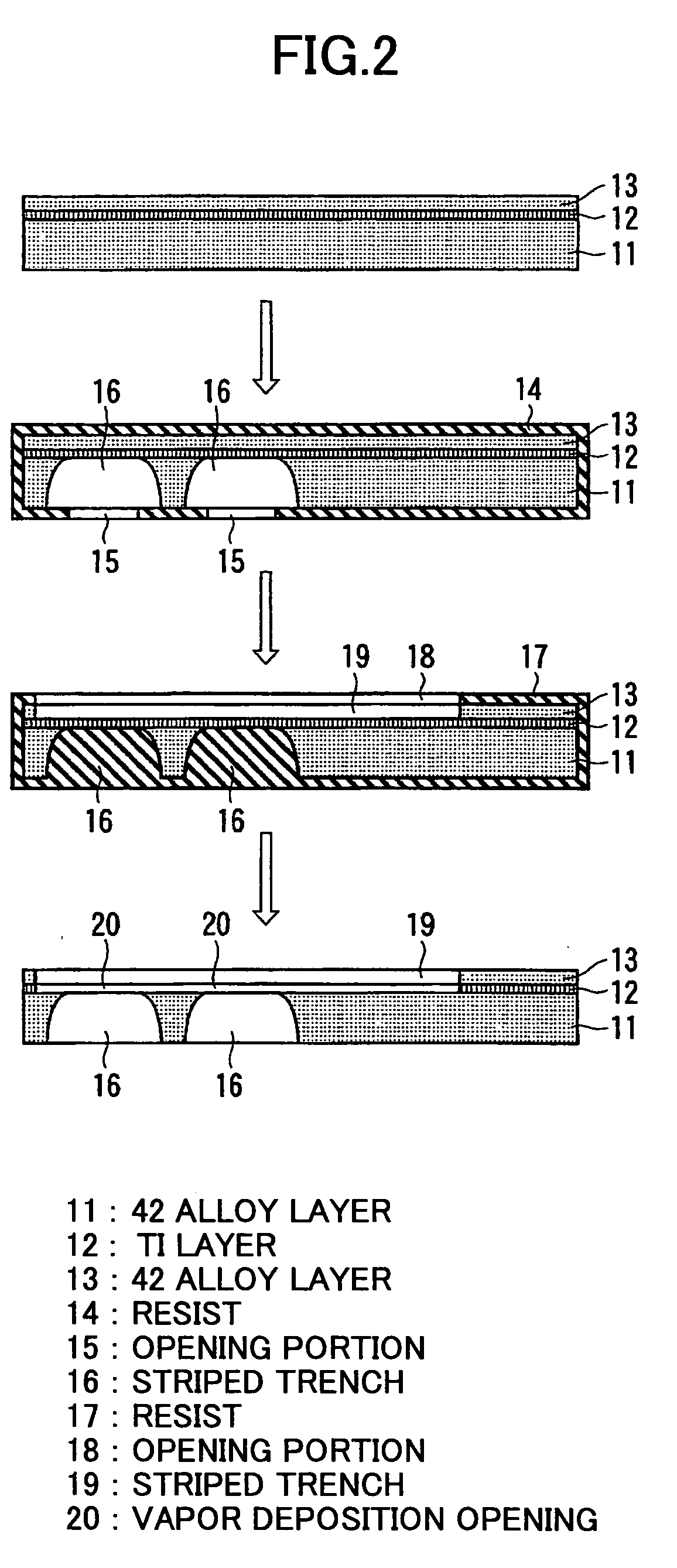
[0051]FIGS. 2 and 3 illustrate a vapor deposition mask according to a first embodiment of the present invention.

[0052] First, referring to FIG. 2, a metal plate member is formed by laminating on a 42 alloy (42 Ni—Fe) layer 11 with a thickness of 40 μm, for example, a Ti layer 12 with a thickness of 1 μm, for example, and then successively laminating a 42 alloy layer 13 with a thickness of 10 μm, for example, on the Ti layer 12.

[0053] Then, after a resist 14 is applied on the front and back surfaces of the metal plate member, plural opening portions 15 with a width of 100 μm are formed at a pitch of 360 μm, for example, to form a striped trench structure corresponding to a pattern of openings extending in the pixel column directions on the 42 alloy layer 11. Then, the resist 14 used to form the opening portions 15 is used as a mask to form striped trenches 16 through an etching process using a ferric chloride solution (50° C. [solution temperature], 47 Be [Baume density]).

[0054] I...

embodiment 2

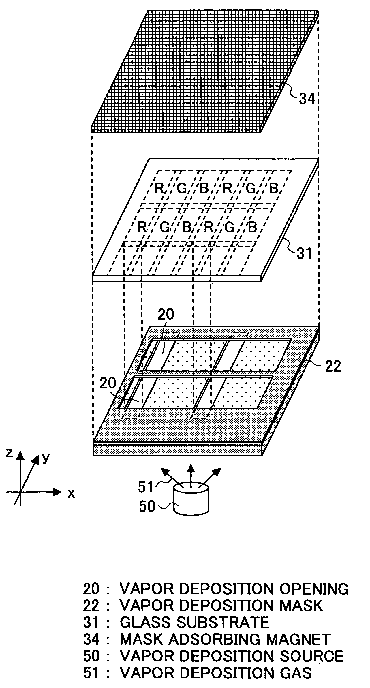
[0060] In the following, an organic EL display device manufacturing method according to a second embodiment of the present invention is described with reference to FIGS. 4 through 7. It is noted that in each of FIGS. 4, 5, and 7, the left side section corresponds to a cross-sectional view across line A-A′ of FIG. 3, and the right side section corresponds to a cross-sectional view across line B-B′ of FIG. 3.

[0061] First, referring to FIG. 4, an ITO film (not shown) having a thickness of 150 nm, for example, is deposited on a glass substrate 31 having a thickness of 0.7 mm, for example, after which anodes 32 having a width of 80 μm are formed at a pitch of 120 μm, for example, through a normal photo etching process.

[0062] In this example, the glass substrate 31 is preferably made of alkali-free glass, which has a thermal expansion coefficient that is close to that of the 42 alloy used for the vapor deposition mask.

[0063] Then, a hole layer vapor deposition mask 33 is positioned to ...

embodiment 3

[0079] In the following, a vapor deposition mask according to a third embodiment of the present invention is described with reference to FIGS. 8 and 9. It is noted that the vapor deposition mask of this embodiment may be manufactured in a manner identical to that for manufacturing the vapor deposition mask according to the first embodiment, and thereby, descriptions of the manufacturing process for the vapor deposition mask of the present embodiment are omitted.

[0080]FIG. 8 is a diagram showing the structure of the vapor mask 52 according to the third embodiment in which the rows of perforated vapor deposition openings 53 are shifted from one another by a pitch corresponding to the dimension (width) of one color pixel.

[0081]FIG. 9 is a perspective diagram showing the deposited states of the light emitting layers. In forming the RGB color light emitting layers according to the present embodiment, a light emitting layer vapor deposition mask 52 is placed on the deposition surface si...


PUM

PropertyMeasurementUnit
thicknessaaaaaaaaaa
thicknessaaaaaaaaaa
thicknessaaaaaaaaaa

Abstract

A vapor deposition mask with high pattern accuracy particularly at vapor deposition openings is realized without changing the substrate structure. The vapor deposition mask includes a plate member, a first concave pattern provided at a first surface of the plate member, a second concave pattern provided at a second surface of the plate member on the opposite side of the plate member, and a through hole pattern provided at meeting or intersecting portions of the first concave pattern and the second concave pattern. The shape of the through hole pattern is arranged to be different from both that of the first concave pattern and that of the second concave pattern.

Description

BACKGROUND OF THE INVENTION [0001] 1. Field of the Invention [0002] The present invention relates generally to a vapor deposition mask and an organic EL display device manufacturing method, and particularly to a vapor deposition mask having an opening portion with high pattern accuracy that is arranged to prevent vapor deposition patterning deviation. [0003] 2. Description of the Related Art [0004] In recent years and continuing, much attention is being directed to organic EL (electroluminescence) display devices to be used in place of liquid crystal display devices in the field of mobile information terminal apparatuses such as mobile phones and mobile PCs. [0005] An organic EL display device includes self-light-emitting pixels that develop electroluminescence on their own, and thereby, a backlight, which is an essential component of a transmissive liquid crystal display device, is not required in an organic EL display device. Also, since an organic EL display device does not use p...

Claims


Application Information

Patent Timeline
Patent Type & Authority Applications(United States)
IPC IPC(8): B05D5/06B05D5/12C23C14/04H05B33/10C23C14/12C23C14/24C23C16/00C23C16/04H01L27/32H01L51/50H05B33/12H05B33/14
CPCC23C14/042H01L51/0011H01L27/3211C23C14/12C23F1/02G03F7/12H10K59/35H10K71/166H05B33/10C23C14/04
Inventor SAKAMOTO, YOSHIAKI
Owner FUJIFILM HLDG CORP
Why Eureka
Try Eureka