Plasma processing device and baffle plate thereof

a processing device and a technology of baffle plate, which are applied in the field of plasma processing device and baffle plate, can solve the problems of difficult control of the inner pressure of the processing region, difficult to keep the pressure of the manifold part constant, and the processing gas inside the processing region b>84/b> cannot be exhausted

Inactive Publication Date: 2005-08-04
TOKYO ELECTRON LTD
View PDF4 Cites 73 Cited by
  • Summary
  • Abstract
  • Description
  • Claims
  • Application Information

AI Technical Summary

Benefits of technology

[0037] In the second embodiment, it is preferred that a distance between the plurality of the protruded portions is substantially twice a thickness of a sheath formed in the vicinity of a baffle member or less, so that equipotential surfaces of a sheath field can be maintained substantially in parallel with a surface normal to a flow direction of a processing gas to be exhausted from the processing region.

Problems solved by technology

And, at the same time, there is a difficulty in controlling an inner pressure of the processing region 84 by way of a CM for pressure control, which is disposed in the manifold part, since it is difficult to keep a pressure of the manifold part constant.
However, the neutral gas particle 41 is not allowed to penetrate through, so that the processing gas inside the processing region 84 cannot be exhausted.
However, the proper range in the diameter of the gas passage hole 86a shown inFIG. 14 is too narrow and varies depending on a condition of the plasma 40, so that the diameter of the gas passage hole 86a cannot be set properly and it is difficult to reliably exhaust the processing gas inside the processing region and at the same time securely suppress the leakage of the plasma.

Method used


Image

  • Plasma processing device and baffle plate thereof
  • Plasma processing device and baffle plate thereof
  • Plasma processing device and baffle plate thereof

Examples


first embodiment

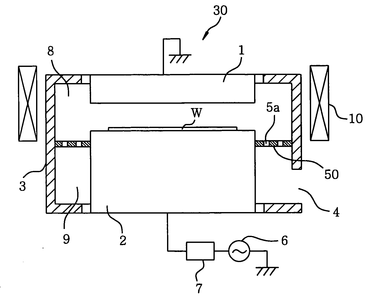
[0068]FIG. 1 is a view for showing a schematic configuration of a plasma processing device in accordance with the present invention.

[0069] As shown in FIG. 1, a magnetron type parallel plate plasma processing device 30 includes a cylindrical processing container 3 that contains an upper electrode 1 and a cylindrical lower electrode 2 in a top part and a lower part thereof, respectively, wherein the lower electrode 2 has a mounting surface in a top part thereof, on which a semiconductor wafer W as a substrate to be processed is mounted. Between the upper electrode 1 and the lower electrode 2, a gap for performing a plasma processing on the semiconductor wafer W is formed. Further, the lower electrode 2 is disposed substantially parallel to the upper electrode 1.

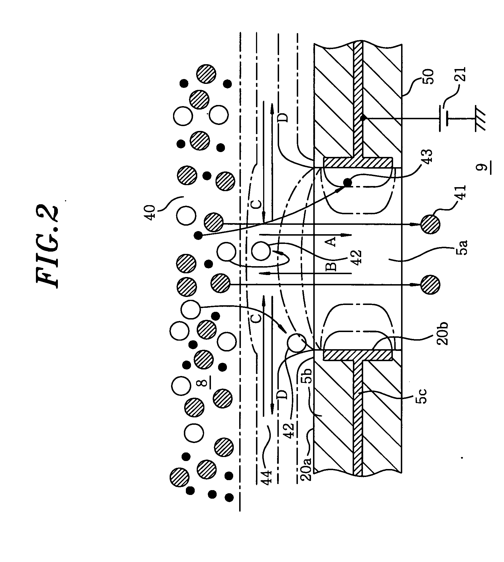
[0070] Still further, the processing container 3 includes a separator 50 (separating unit, baffle plate) for dividing an inside thereof into a processing region 8 and an exhaust region 9, in the vicinity of the lower electrod...

second embodiment

[0081]FIG. 3 shows a schematic configuration of a plasma processing device in accordance with the present invention.

[0082] Since a configuration of the second embodiment is basically same as that of the first embodiment, like reference numerals will be assigned to like parts having substantially same functions and redundant description thereof will be omitted. Hereinafter, other parts will be explained only.

[0083] As shown in FIG. 3, a magnetron type parallel plate plasma processing device 30 includes a wavy baffle member 50′ (separating unit, baffle plate) for dividing an inside of a processing container 3 into a processing region 8 and an exhaust region 9.

[0084]FIG. 4 is a cross sectional view of the wavy baffle member 50′ in FIG. 3.

[0085] As shown in FIG. 4, the wavy baffle member 50′ is of a curved wave shape such that curved portions 71 and 72 thereof are alternately formed in the processing region 8 and in the exhaust region 9. The wavy baffle member 50′ has in each of slop...

third embodiment

[0089]FIG. 5 shows a schematic configuration of a plasma processing device in accordance with the present invention.

[0090] Since a configuration of the third embodiment is basically same as that of the first embodiment, like reference numerals will be assigned to like parts having substantially same functions and redundant description thereof will be omitted. Hereinafter, other parts will be explained only.

[0091] As shown in FIG. 5, a magnetron type parallel plate plasma processing device 30 includes a multi-layered baffle member 50″ (separating unit, baffle plate) for dividing an inside of a processing container 3 into a processing region 8 and an exhaust region 9. As shown in FIG. 6, the multi-layered baffle member 50″ contains a plurality of first blade shaped baffle plates 51 provided in an outer periphery of a lower electrode 2 with equiangular spaces therebetween, and a plurality of second blade shaped baffle plates 52 provided in an inner periphery of the processing containe...


PUM

PropertyMeasurementUnit
ionization energyaaaaaaaaaa

Abstract

A plasma processing device able to positively enhance a process-gas exhaust efficiency in a processing region and restrict plasma leaking. A processing container of a magnetron type parallel plate plasma processing device has a separator for separating the inside of the processing container into a processing region and an exhaust region. The separator has a plurality of gas passage holes to establish communication between the processing region and the exhaust region, and includes a non-conductive member. A conductive member is disposed on a gas passage-side surface facing the gas passage holes. A voltage V is applied by a power supply to the conductive member so that the gas passage-side surface is at a potential higher than that of a processing-region surface.

Description

FIELD OF THE INVENTION [0001] The present invention relates to a plasma processing device and a baffle plate thereof; and, more particularly, to a plasma processing device and a baffle plate thereof for performing a processing such as an etching, a surface modification, a thin film forming, or the like. BACKGROUND OF THE INVENTION [0002] In a recent trend of miniaturization of a semiconductor device, a processing technology having a high degree of accuracy on a semiconductor wafer is required. For performing a high accuracy microprocessing on the semiconductor wafer, e.g., a plasma etching processing, a magnetron type parallel plate plasma processing device has been commonly used. [0003]FIG. 13 offers a schematic configuration of a magnetron type parallel plate plasma processing apparatus of a conventional art. [0004] As shown in FIG. 13, a plasma processing apparatus 80 includes a processing container 81, and the processing container 81 contains an upper electrode 82 and a lower el...

Claims


Application Information

Patent Timeline
Patent Type & Authority Applications(United States)
IPC IPC(8): H05H1/46B01J19/08C23C16/455C23C16/50H01J37/32H01L21/205H01L21/3065
CPCH01J37/32834H01J37/32633B01J19/08H01L21/3065
Inventor ISHIHARA, HIROYUKIARAKI, YOUICHITAKAHASHI, TOSHIKIKUBO, TAKUYAITO, ATSUSHIONO, YOKO
Owner TOKYO ELECTRON LTD
Why Eureka
Try Eureka