Nitride semiconductor thin film and method for growing the same

a technology of semiconductor thin film and nano-nitride, which is applied in the direction of crystal growth process, semiconductor laser, polycrystalline material growth, etc., can solve the problems of large number of defects such as threading dislocation and degradation of device properties, and achieve high quality

Inactive Publication Date: 2005-08-04
LG ELECTRONICS INC
View PDF1 Cites 9 Cited by
  • Summary
  • Abstract
  • Description
  • Claims
  • Application Information

AI Technical Summary

Benefits of technology

[0012] The present invention is conceived to solve the aforementioned problems. Accordingly, an object of the present invention is to provide a nitride semiconductor thin film and a method for growing the same, wherein a plurality of grooves are formed on a substrate by partially etching the ...

Problems solved by technology

However, since nitride semiconductor thin films and sapphire substrates have large differences in the lattice constants and the coefficients of thermal expansion, there are disadvant...

Method used


Image

  • Nitride semiconductor thin film and method for growing the same
  • Nitride semiconductor thin film and method for growing the same
  • Nitride semiconductor thin film and method for growing the same

Examples


Embodiment Construction

[0021] Hereinafter, a preferred embodiment of the present invention will be described in detail with reference to the accompanying drawings.

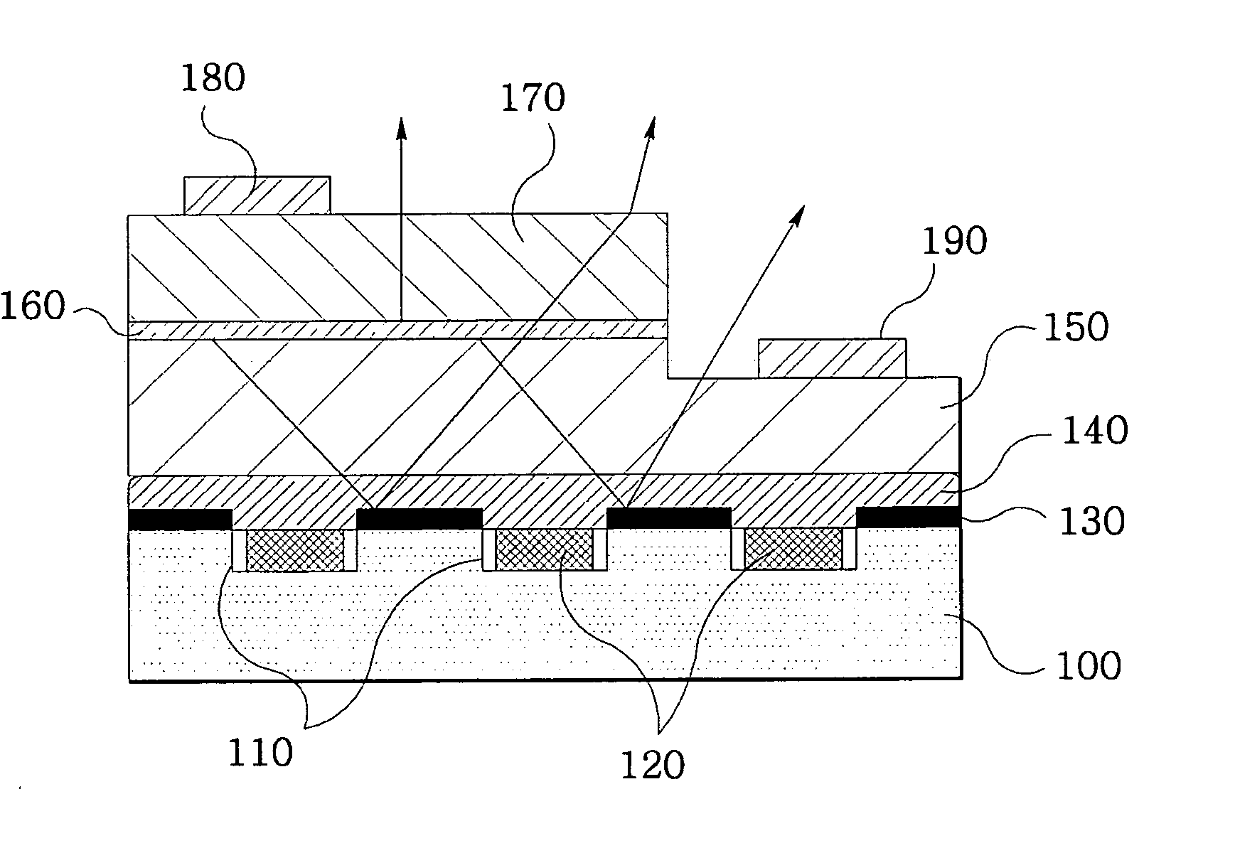
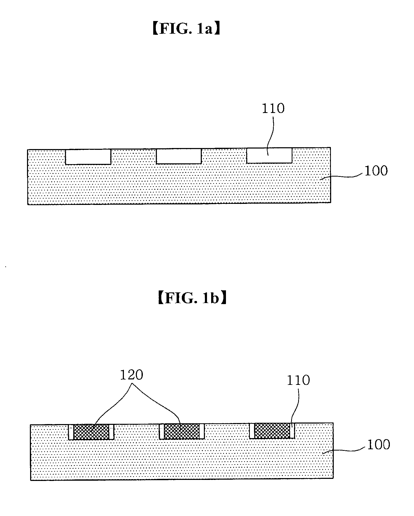
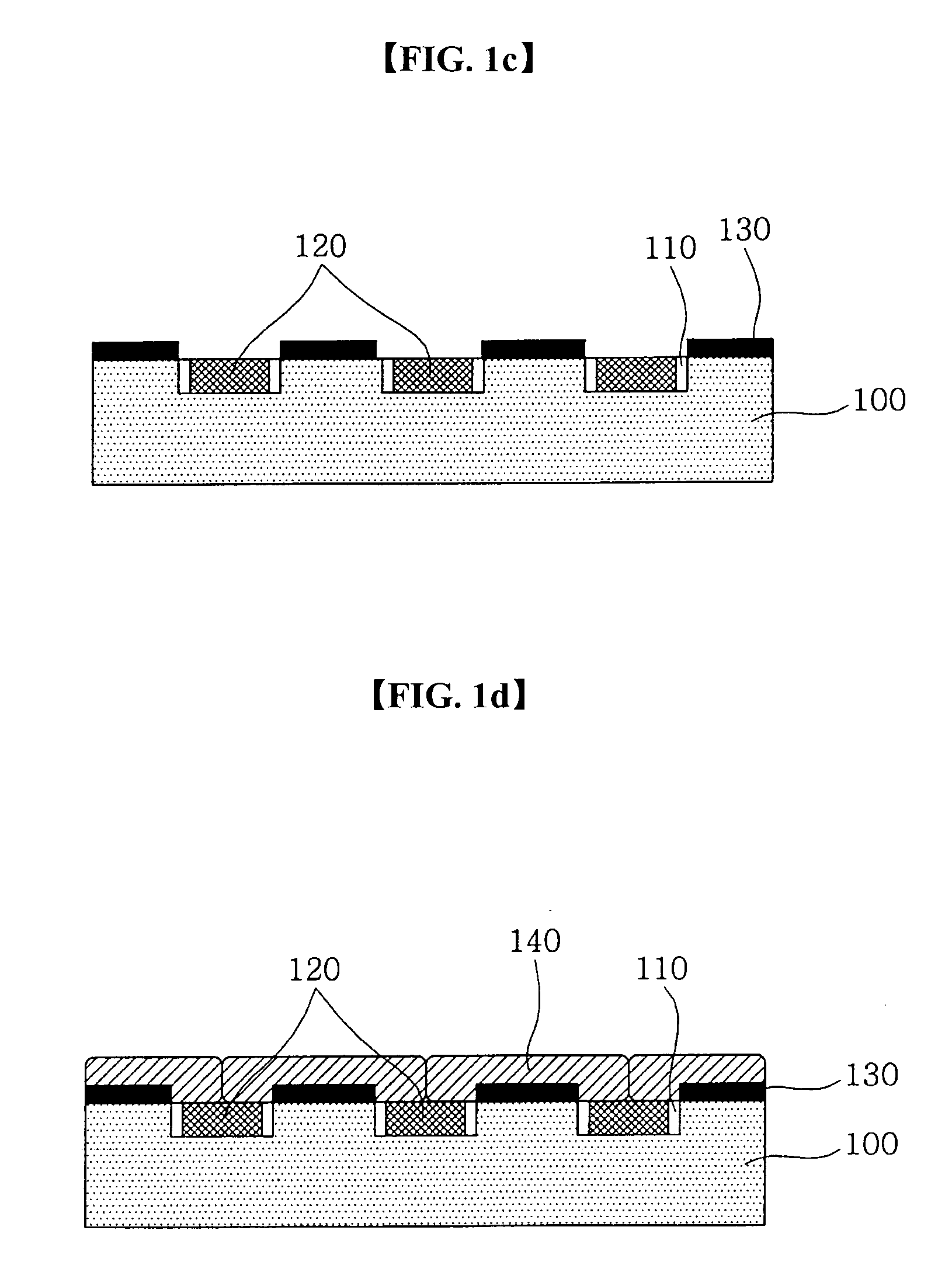
[0022]FIGS. 1a to 1d are views illustrating a process of growing a high quality nitride semiconductor thin film according to the present invention. First, a plurality of grooves 110 are formed in a top surface of a sapphire substrate 100 by partially etching the sapphire substrate 100 (FIG. 1a).

[0023] Here, the top surface of the sapphire substrate 100 has a corrugated shape.

[0024] Thereafter, a leg portion 120 for preventing longitudinal growth of a nitride semiconductor is formed within each of the grooves 110 formed in the sapphire substrate 100 (FIG. 1b).

[0025] At this time, the leg portion 120 is constructed of an oxide film or nitride film such as SiO2, Si3N4, TiOx or ZrOx, or a multi-layered film comprising such oxide and nitride films.

[0026] Further, the leg portion 120 is constructed of a film made of one selected from the group co...


PUM

PropertyMeasurementUnit
Fractionaaaaaaaaaa
Widthaaaaaaaaaa
Areaaaaaaaaaaa

Abstract

The present invention relates to a nitride semiconductor thin film and a method for growing the same. The present invention has an advantage in that a plurality of grooves are formed on a substrate by partially etching the substrate, and leg portions for preventing longitudinal growth of a nitride semiconductor are formed within the grooves so that the nitride semiconductor thin film is grown laterally to cover top portions of the leg portions, thereby ensuring growth of a high quality nitride semiconductor thin film.

Description

BACKGROUND OF THE INVENTION [0001] 1. Field of the Invention [0002] The present invention relates to a nitride semiconductor thin film and a method for growing the same. More particularly, the present invention relates to a nitride semiconductor thin film and a method for growing the same, wherein a plurality of grooves are formed on a substrate by partially etching the substrate, and leg portions for preventing longitudinal growth of a nitride semiconductor are formed within the grooves so that the nitride semiconductor thin film is grown laterally to cover top portions of the leg portions, thereby ensuring growth of a high quality nitride semiconductor thin film. [0003] 2. Description of the Related Art [0004] Generally, nitride-based semiconductors are direct transition type semiconductors and have been applied to light emitting elements such as light emitting diodes (LEDs) and laser diodes (LDs). Further, studies on application of the semiconductors to high temperature, high fre...

Claims


Application Information

Patent Timeline
IPC IPC(8): C30B25/18C23C16/34C30B29/40H01L21/20H01L21/205H01L21/36H01L33/12H01L33/32H01S5/323
CPCC30B25/183C30B29/403H01L21/0237H01L21/02647H01L21/0254H01L21/02639H01L21/02642H01L21/02458H01L21/34
Inventor SEO, JUNG HOON
Owner LG ELECTRONICS INC
Why Eureka
Try Eureka