Semiconductor module

a technology of semiconductor modules and modules, applied in the direction of semiconductor devices, semiconductor/solid-state device details, electrical apparatus, etc., can solve problems such as operation errors or malfunctions, voltage drop-down can occur, and circuitry cannot supply the required voltag

Inactive Publication Date: 2005-08-04
KK TOSHIBA
View PDF18 Cites 74 Cited by
  • Summary
  • Abstract
  • Description
  • Claims
  • Application Information

AI Technical Summary

Problems solved by technology

A form having a single power supply unit for supplying electrical power to a plurality of circuits is such that a voltage drop-down can occur even due to the presence of tiny parasitic impedance of wiring lines.
This voltage drop might lead to a failure in supplying a required voltage to circuitry, which in turn causes operation errors or malfunctions.
In most cases, a power device such as the power MOSFET used in power supply circuitry experiences heatup, which is caused by power losses due to turn-on resistance and switching operations.

Method used


Image

  • Semiconductor module
  • Semiconductor module
  • Semiconductor module

Examples


first embodiment

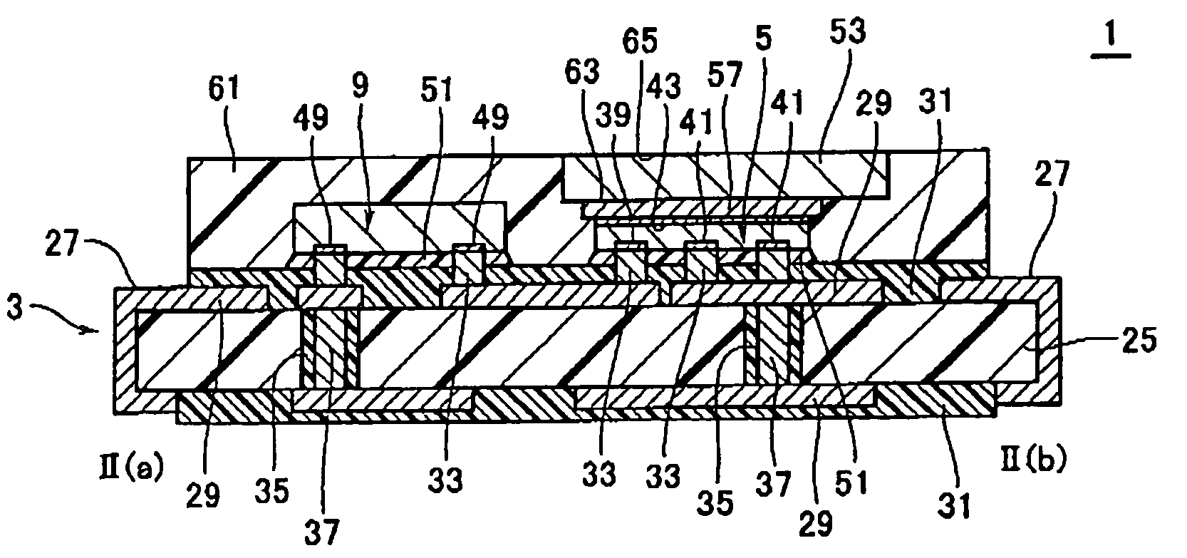
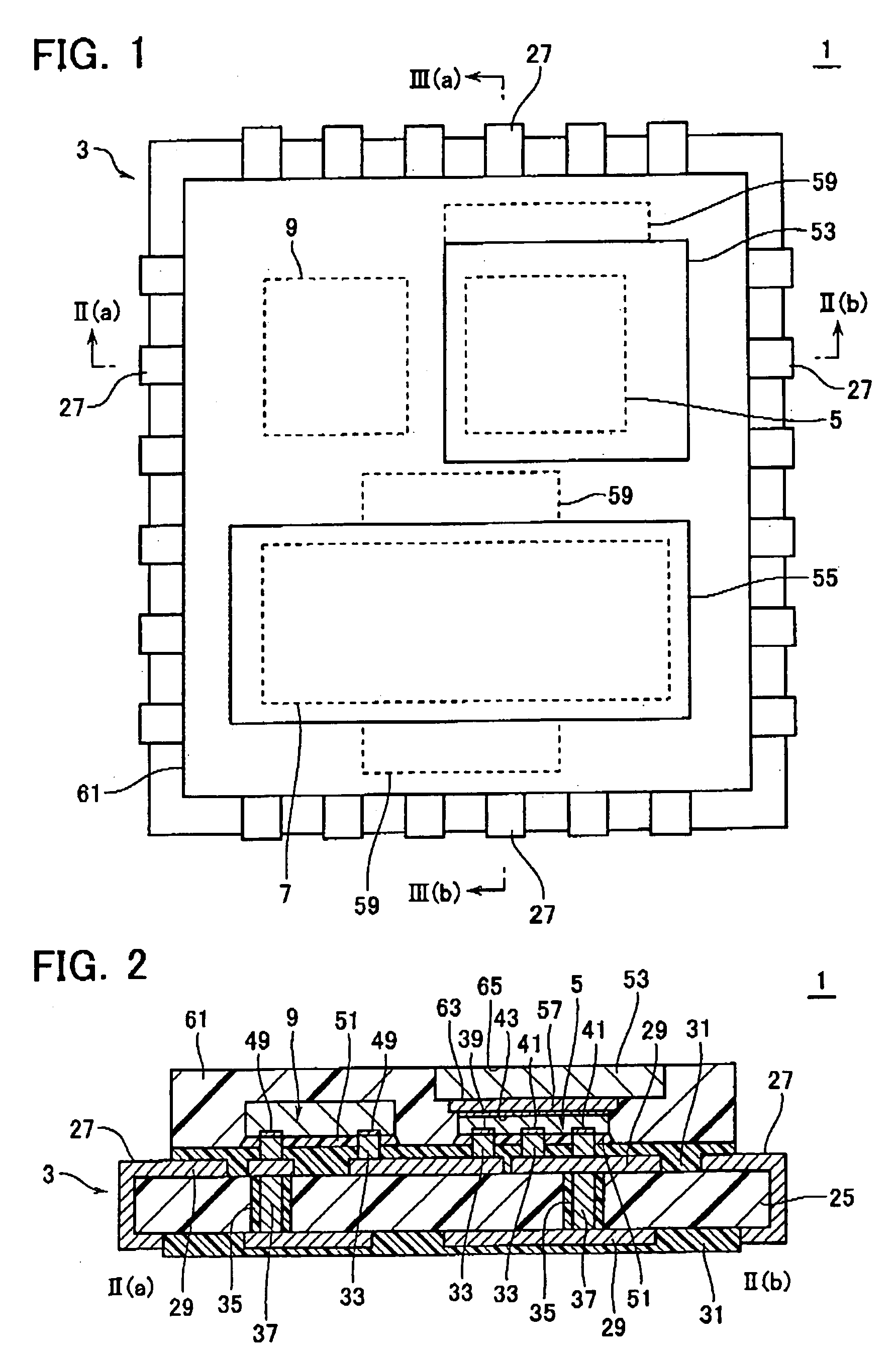
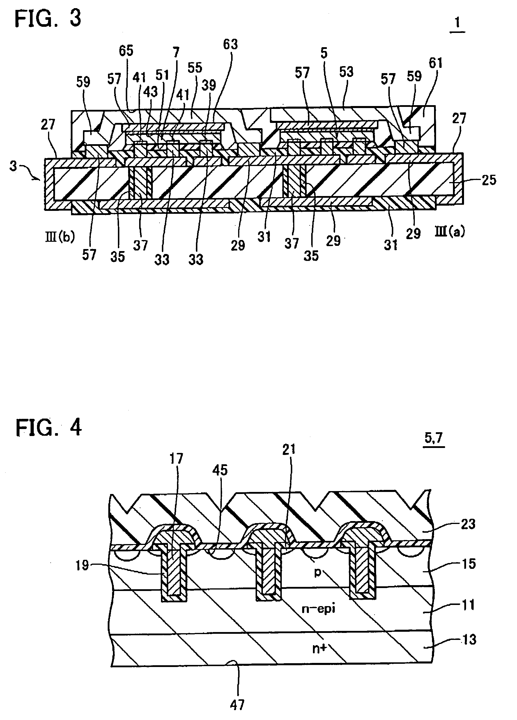
[0028] The structure of a semiconductor module in accordance with a first embodiment of the invention will be explained with reference to FIGS. 1 to 3. FIG. 1 is a plan view of the semiconductor module in accordance with the first embodiment. FIG. 2 is a cross-sectional diagram of the module as taken along line II(a)-II(b) of FIG. 1, whereas FIG. 3 is a sectional view taken along line III(a)-III(b) of FIG. 1.

[0029] The semiconductor module 1 has a parts-mounting or packaging substrate (for example, printed wiring board) 3 and IC chips mounted thereon, wherein the chips include two power MOS chips 5 and 7 and an IC chip 9 for drive use. The driver IC chip 9 is for driving the gates of MOSFETs formed on the power MOS chips 5 and 7.

[0030]FIG. 4 shows a sectional view of part of the power MOS chip 5, 7. The chip 5, 7 is structured so that a great number of vertical type MOSFETs are connected in parallel with one another. Explaining in more detail, the chip 5, 7 has a heavily-doped n (...

second embodiment

[0062]FIG. 8 is a diagram showing a plan view of a semiconductor module 81 in accordance with a second embodiment of the invention. FIG. 9 is a cross-sectional diagram of the module of FIG. 8 as taken along line IX(a)-IX(b). The second embodiment will be set forth with reference to FIGS. 8-9 while focusing an explanation on its differences from the first embodiment.

[0063] In the second embodiment, the heat sink 53 that covers the power MOS chip 5 extends to overlie the driver IC chip 9, thereby covering the driver IC chip 9. This permits the power MOS chip 5 and the driver IC chip 9 to commonly use or “share” the heat sink 53. Accordingly, the heat sink is allowed to have a larger area when compared to the case where a separate heat sink covering the driver IC chip 9 is laid out in addition to the heat sink 53. This makes it possible to improve the heat releasability by a degree corresponding thereto.

[0064] Note however that the back face 83 of driver IC chip 9 stays at ground pot...

third embodiment

[0068] A third embodiment is different from the embodiments stated above in that the former is equipped with a power MOS chip (synchronous rectification-side element) 7 with a built-in SBD 69. FIG. 10 illustrates, in cross-section, part of the power MOS chip (synchronous rectification-side element) 7 equipped in the third embodiment, which corresponds to FIG. 4. The SBD 69 Is formed so that it is spaced apart by a specified distance from a terminate end 85 of a MOSFET fabrication region. This specified distance is a distance which avoids any appreciable interference between the MOSFET and SBD.

[0069] The SBD 69 is configured from an epitaxial layer 11 and a metallic film 87 made of aluminum or the like, which is formed thereon. The epitaxial layer 11 and metal film 87 are contacted together, resulting in formation of a Schottky barrier at such contact portion. SBD 69 is connected In parallel to the MOSFET of power MOS chip 7. The SBD 69 may be replaced with a pn-junction diode when ...


PUM


Abstract

A semiconductor module includes a parts-mounting or packaging substrate, a plurality of power metal insulator semiconductor (MIS) chips which have top surfaces and back surfaces and are mounted by flip chip bonding on or above the package substrate while letting the top-surfaces face the package substrate, a drive-use integrated circuit (IC) chip which is mounted by flip chip bonding above the package substrate for driving the gates of metal insulator semiconductor field effect transistors (MISFETs) that are formed on the power MIS chips a plurality of heat sinks disposed on or above the back surfaces of the power MXS chips, and a resin member for sealing the power MIS chips and the driver IC chip together in a single package.

Description

CROSS-REFERENCE TO RELATED APPLICATIONS [0001] This application is based upon and claims the benefit of priority from the prior Japanese Patent Application No. 2004-027066, filed on Feb. 3, 2004, the entire contents of which are incorporated herein by reference. BACKGROUND OF THE INVENTION [0002] 1. Field of the Invention [0003] The present invention relates to semiconductor modules such as multi-chip modules, for example. [0004] 2. Description of the Related Art [0005] DC-to-DC converters are the devices that convert a DC current at one voltage into a DC current with a different voltage level. As DC-DC converters are of high efficiency and are designable to have small sizes, these are adaptable for use as power supply units to be built in various types of small-size electronic equipment (for example, information communication equipment such as notebook personal computers or “PCs” and handheld wireless telephone handsets, also known as mobile phones). [0006] Information communicatio...

Claims


Application Information

Patent Timeline
Patent Type & Authority Applications(United States)
IPC IPC(8): H01L25/07H01L21/56H01L23/31H01L23/34H01L23/433H01L25/16H01L25/18
CPCH01L21/563H01L23/3121H01L2924/12032H01L2224/73204H01L2224/32225H01L2224/16225H01L2924/3025H01L2924/3011H01L2924/19041H01L23/4334H01L25/165H01L2224/16H01L2224/73253H01L2924/13055H01L2924/13091H01L2924/16152H01L2924/00H01L2224/05571H01L2224/05573H01L2224/32245H01L2924/00014H01L2224/05599
Inventor SATO, NOBUYUKI
Owner KK TOSHIBA
Why Eureka
Try Eureka