Method for lowering noise and providing offset correction in a transimpedance amplifier

a transimpedance amplifier and offset correction technology, applied in the direction of electric/magnetic computing, instruments, computation operations for integration/differentiation, etc., can solve the problems of lower bit error rate (bers) and additional noise in the design of the transimpedance amplifier, and achieve the effect of reducing noise enhancemen

Inactive Publication Date: 2005-08-04
AVAGO TECH WIRELESS IP SINGAPORE PTE
View PDF33 Cites 7 Cited by
  • Summary
  • Abstract
  • Description
  • Claims
  • Application Information

AI Technical Summary

Benefits of technology

[0007] The present invention provides a system including an input device (e.g., a photodetector), an amplification device, and a feedback device. The amplification device receives a signal from the input device and includes a transimpedance portion that converts the input current to a voltage. The transimpedance portion includes a first section having a plurality of elements (e.g., resistors and transistors) and a second section having a plurality of elements (e.g., resistors and transistors). The elements (e.g., transistors and resistors) in the first and second sections are mismatched to introduce a systematic offset in the transimpedance stage to make a net input offset at the amplification device unidirectional. The feedback device (e.g., an integrator) can be coupled to an output of the amplification device and an input of the transimpedance portion to provide a single ended unidirectional offset correction to the amplification device for reduced noise enhancement.

Problems solved by technology

This results in lower bit error rates (BERs) when the TIAs are used in optical receiving devices (e.g., photodetectors, optical sensors, optical detectors, or the like).
Unfortunately, the feedback device results in additional noise in the design of the transimpedance amplifier.

Method used


Image

  • Method for lowering noise and providing offset correction in a transimpedance amplifier
  • Method for lowering noise and providing offset correction in a transimpedance amplifier
  • Method for lowering noise and providing offset correction in a transimpedance amplifier

Examples


Embodiment Construction

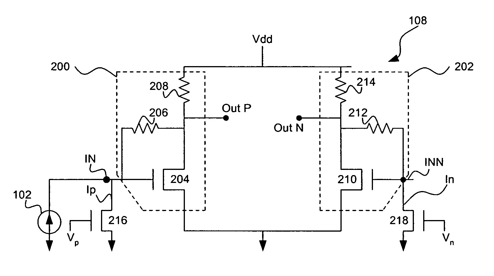
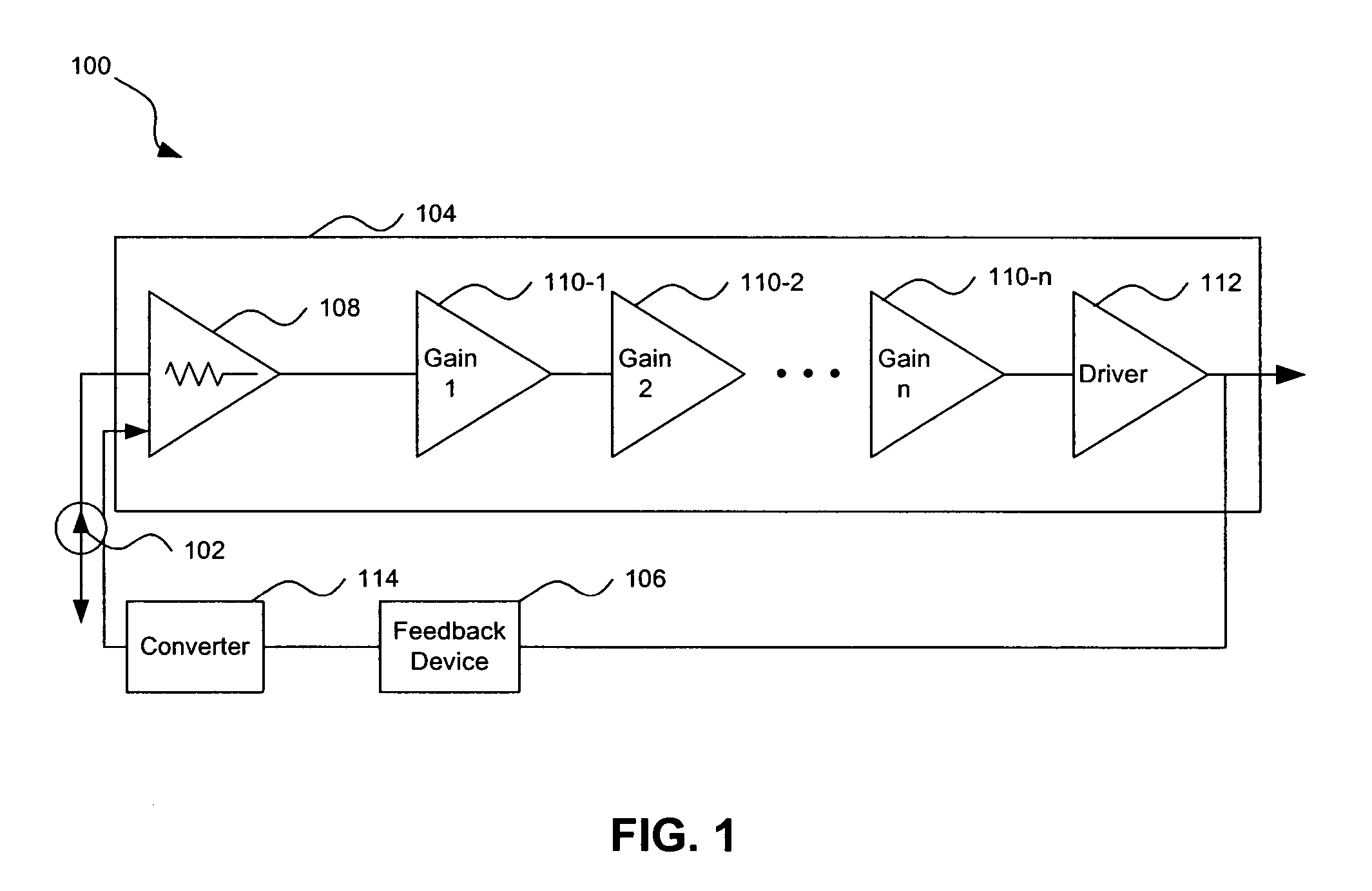
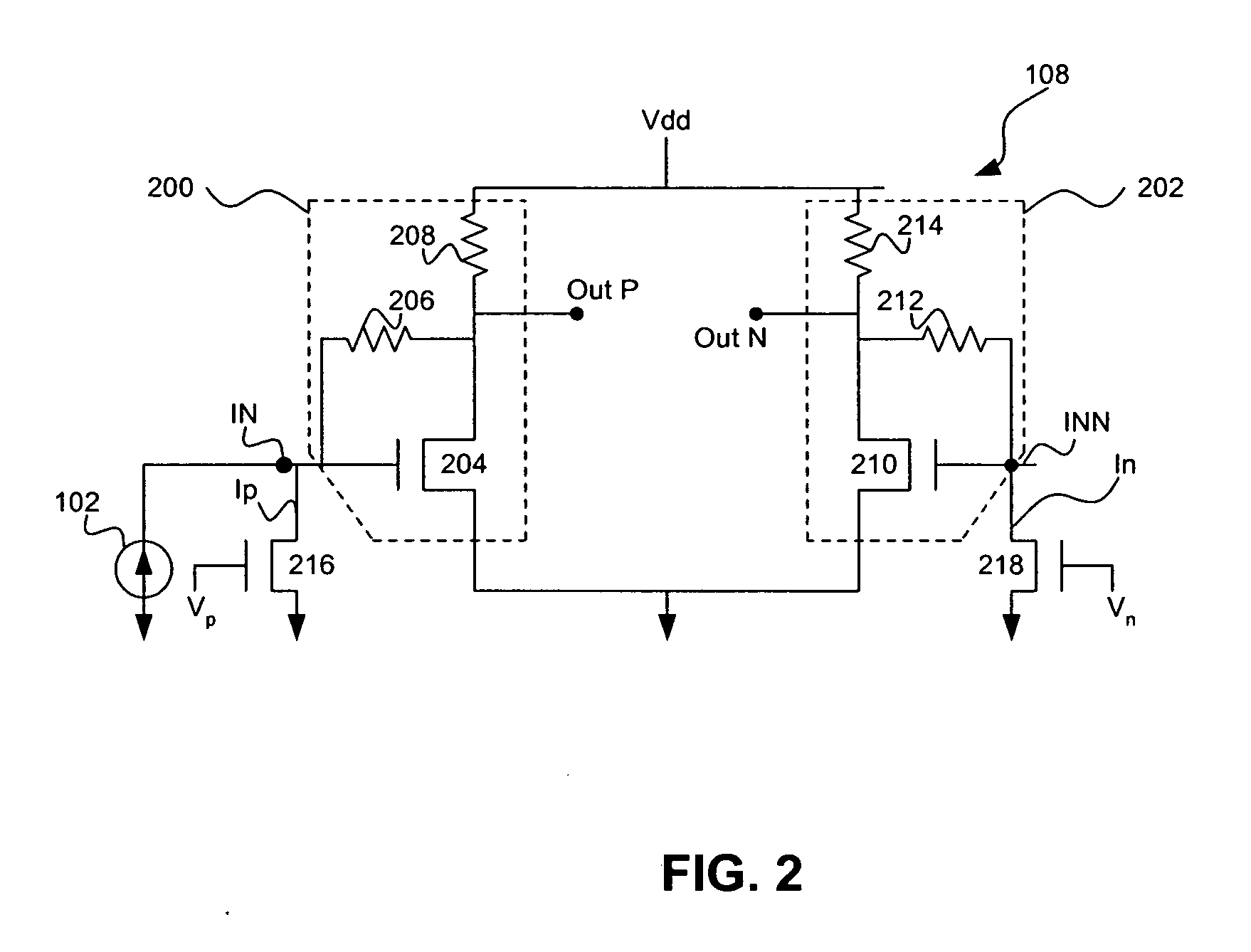
[0017]FIG. 1 shows a system (e.g., an optical receiving system) 100 according to embodiments of the present invention. System 100 includes an optical receiving device (e.g., photodetector, optical detector, or optical sensor) 102 that feeds a signal (e.g., a current) into a transimpedance amplifier (TIA) 104, which converts the signal to a voltage signal and amplifies the signal for later processing. In some embodiments, the signal is a current based on an optical signal detected by optical receiving device 102. TIA 104 feeds back an output signal through a feedback device (e.g., a D.C. loop circuit or an integrator) 106 to an input of the TIA 104. TIA 104 can include a first stage (e.g., a transimpedance stage) 108, first through n second stages (e.g., gain stages) 110-1 to 110-n, and a third stage (e.g., a driver device or stage) 112. There can also be a converter (e.g., a voltage to current (V / I) converter) 114 positioned between feedback device 106 and TIA 104.

[0018] In some em...


PUM


Abstract

A system for receiving signals (e.g., optical signals) includes an input device, an amplification device, and a feedback device. The amplification device receives a signal from the input device and includes a transimpedance portion. The transimpedance portion includes a first section having a plurality of elements (e.g., resistors and transistors) and a second section having a plurality of elements (e.g., resistors and transistors). One or more of the elements (e.g. transistors or resistors) in the first and second sections are mismatched to introduce a systematic offset in the transimpedance stage, to make the net input referred offset of the amplification device unidirectional. The feedback device (e.g. an integrator) is coupled to an output of the amplification device and an input of the transimpedance portion to provide a unidirectional offset correction to the amplification device for reduced noise enhancement.

Description

CROSS-REFERENCE TO RELATED APPLICATIONS [0001] The application is a continuation if U.S. Ser. No. 10 / 227,257, filed Aug. 26, 2002, which is incorporated by reference herein in its entirety.BACKGROUND OF THE INVENTION [0002] 1. Field of the Invention [0003] The present invention is directed to using offset correction to lower noise in a transimpedance stage of an amplifier. [0004] 2. Background Art [0005] Transimpedance amplifiers (TIAs) and limiting amplifiers (LAs) are typically used in optical receivers, and other devices. The are positioned at front end stages of a system to convert current from a detector (e.g., a photodetector) to voltage output, which is then fed to a clock and data recovery (CDR) circuit. TIAs in high speed communications (e.g., 10 GHz / s baud rates) are often faced with stringent requirements for reducing the input referred noise. This is needed to maximize the signal-to-noise ratio (SNR) of the TIAs. This results in lower bit error rates (BERs) when the TIAs...

Claims


Application Information

Patent Timeline
Patent Type & Authority Applications(United States)
IPC IPC(8): H03F3/08H03F3/45
CPCH03F3/082H03F3/45973H03F3/45748H03F3/087
Inventor GUPTA, SANDEEP K.
Owner AVAGO TECH WIRELESS IP SINGAPORE PTE
Why Eureka
Try Eureka