

Display device
a display device and display technology, applied in the field of display devices, can solve the problems of inability to achieve uniform display, and achieve the effect of suppressing the occurrence of horizontal stripes and improving display quality
- Summary
- Abstract
- Description
- Claims
- Application Information
AI Technical Summary
Benefits of technology
Problems solved by technology
Method used
Image

Examples
embodiment 1
[0051] A liquid crystal display (LCD) according to EMBODIMENT 1 includes a TFT substrate, a CF (color filter) substrate disposed so as to face the TFT substrate and a liquid crystal layer interposed between the substrates and including a nematic liquid crystal material or the like. The CF substrate includes color filter layers of three colors, i.e., red, green and blue, a common electrode made of ITO (indium tin oxide) or the like which covers the color filter layers and a liquid crystal alignment film which covers the common electrode. The color filter layers may be formed on the TFT substrate.
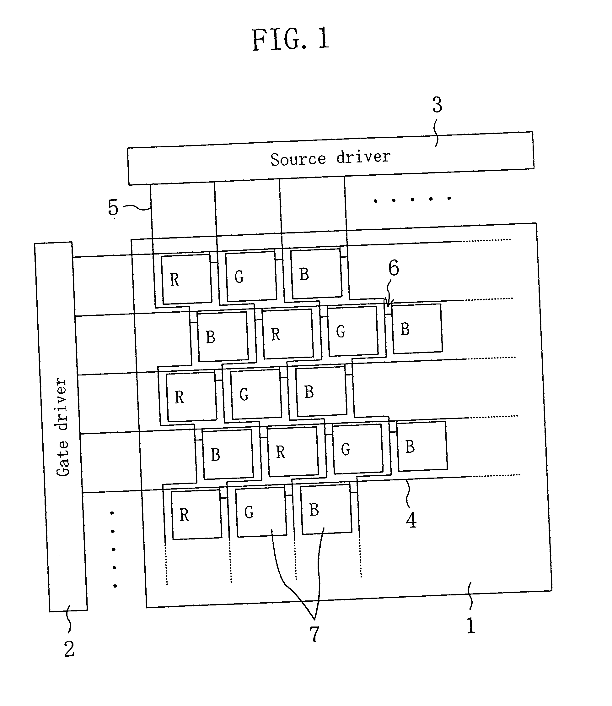
[0052] The TFT substrate of this embodiment will be described with reference to FIG. 1. In a display section 1 of the TFT substrate, a plurality of gate lines 4 each extending from a gate driver 2 and a plurality of source lines 5 each extending from a source driver 3 are formed. A plurality of TFTs 6 as switch elements are formed so that each of the TFTs 6 is located in the vicinity of an i...
embodiment 2
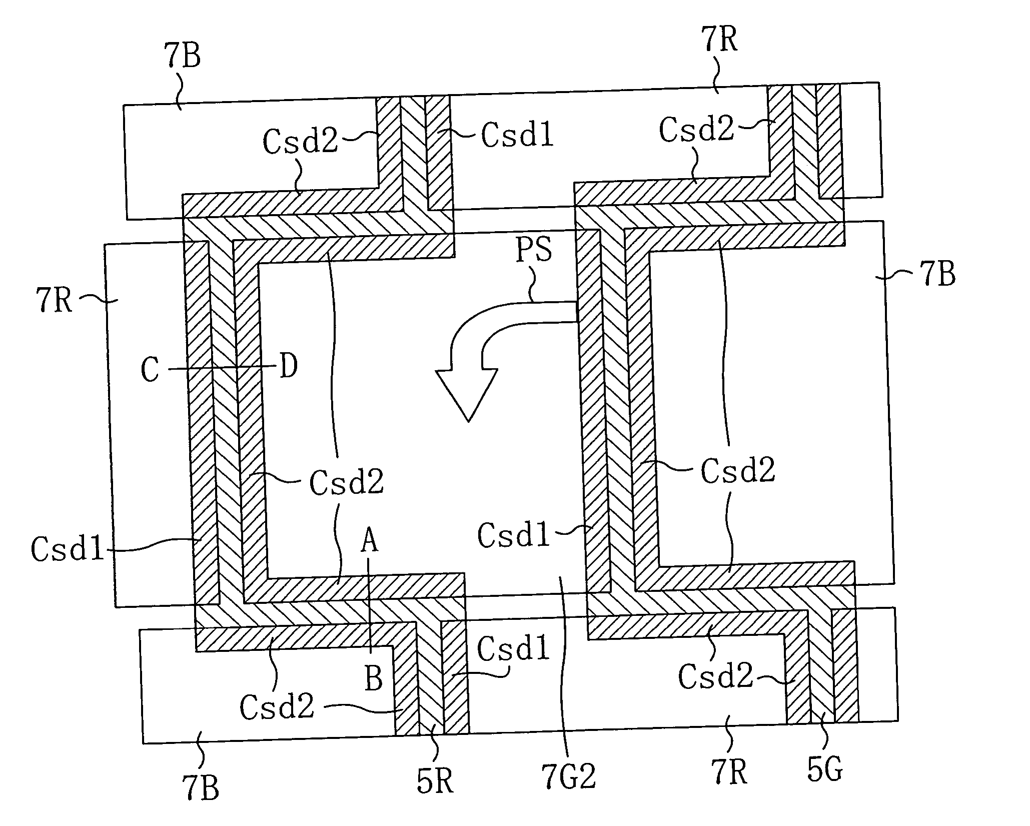
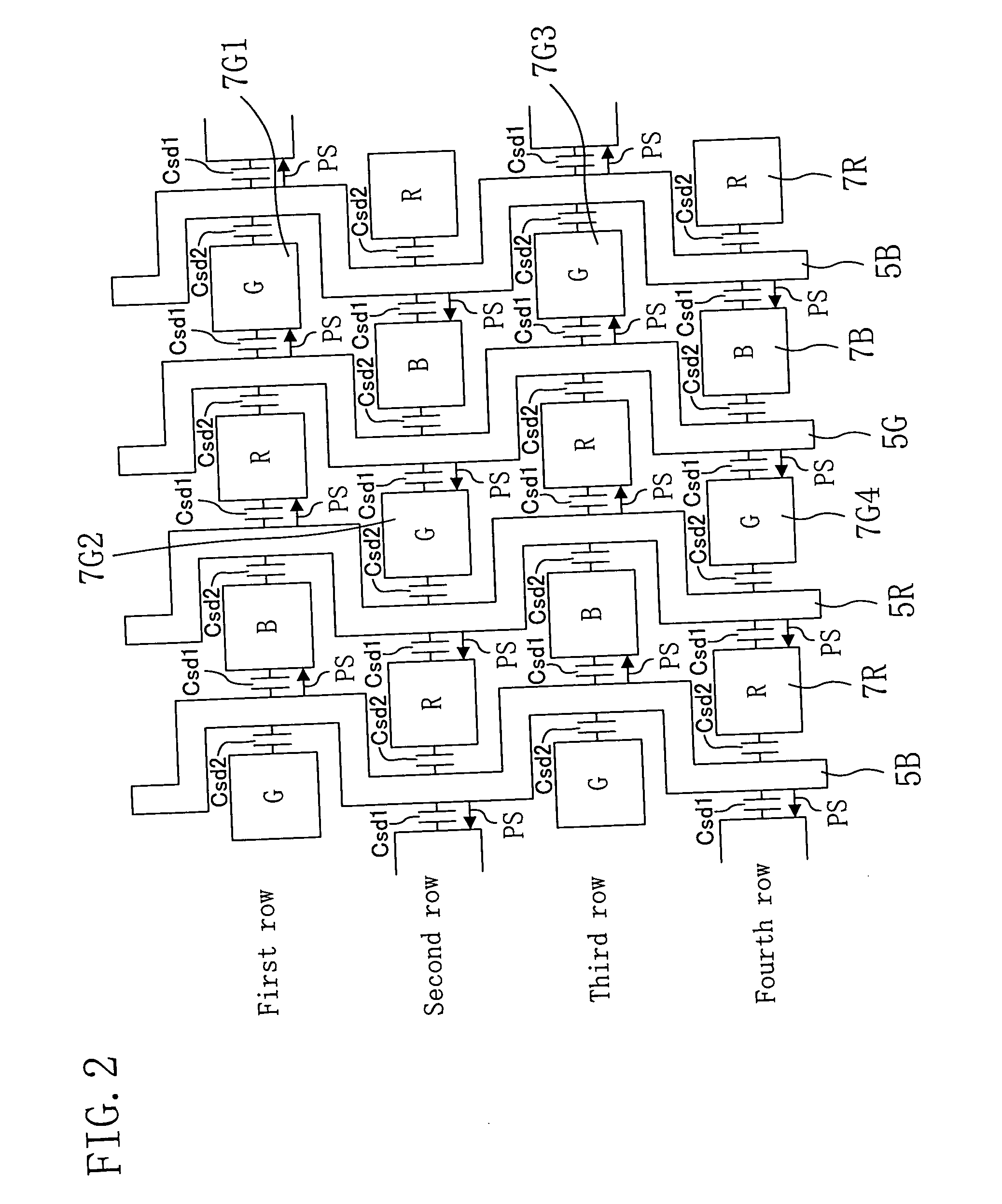
[0069] An LCD according to EMBODIMENT 2 includes, as the LCD of EMBODIMENT 1, a TFT substrate, a CF substrate disposed so as to face the TFT substrate and a liquid crystal layer interposed between the substrates. The LCD of this embodiment has the similar structure to that of the LCD of EMBODIMENT 1, except for the TFT substrate. FIG. 16 is an enlarged plan view illustrating a pixel on the TFT substrate of this embodiment. In FIG. 16, each component of the TFT substrate having substantially the same function as that of the TFT substrate of EMBODIMENT 1 is identified by the same reference numeral and therefore the description thereof will be omitted.
[0070] In the TFT substrate of this embodiment, the signal lines 5 extending in the column direction are disposed so that each of the signal lines 5 is interposed between adjacent two of the pixel electrodes 7 in the row direction and located closer to one of the adjacent two of the pixel electrodes 7 which is driven by the signal line 5...
embodiment 3
[0073] In the LCD of EMBODIMENT 2, each of the pixel electrodes 7 and associated ones of the source lines 5 which do not drive the pixel electrode 7 overlap in the row direction. However, to reduce the capacitance Csd2 as much as possible, each pixel electrode and source lines which do not drive the pixel electrode preferably do not overlap. FIG. 17 is an enlarged plan view illustrating a pixel on the TFT substrate of this embodiment. In FIG. 17, each component of the TFT substrate having substantially the same function as that of the TFT substrate of EMBODIMENT 1 is identified by the same reference numeral and therefore the description thereof will be omitted.
[0074] In the TFT substrate of this embodiment, part of the signal line 5 extending in the column direction and one of adjacent two pixel electrodes 7 with the signal line 5 interposed therebetween in the row direction overlap, but the signal line 5 and the other one of the adjacent two pixel electrodes 7 do not overlap. This...
PUM
 Abstract
Description
Claims
Application Information