Aliasing data processing registers

a data processing register and register technology, applied in the field of data processing systems, can solve the problems of reducing the benefits achieved by simd operation, and achieve the effect of simplifying and speeding up the decoding of the register field

Active Publication Date: 2005-08-04
ARM LTD
View PDF55 Cites 54 Cited by
  • Summary
  • Abstract
  • Description
  • Claims
  • Application Information

AI Technical Summary

Benefits of technology

[0013] The present invention recognises that SIMD data elements stored within a register data store can be accessed more flexibly and accordingly with a reduced need for dedicated data element rearrangement operations if the instructions are allowed to specify the data element size and the register size and register accessing logic is provided which maps a particular register to a portion of the register data store in dependence upon the register size. Thus, an individual data element may be written to a particular point within the register data store as part of the contents of one register of a particular register size, but then read from that same position as part of a different register having a different register size and possibly a different data element size. Registers of differing sizes are effectively aliased on top of each other in a manner which advantageously allows highly flexible access to the data elements without incurring overhead in rearranging those data elements.
[0014] It will be appreciated that a data processing instruction may specify one or more source registers and / or one or more destination registers. The register size and data element size of these different source and destination registers may be independently specified by the data processing instruction. Alternatively, instruction encoding space may be saved by requiring particular relationships between register sizes and element sizes. These relationships can be targeted at those commonly encountered so that flexibility is not unduly reduced.
[0015] A particularly advantageous use of the present technique is one in which the destination data element size differs from one or more of the source data element sizes. This situation commonly arises in SIMD processing operations whereby the data width is increased as a consequence of the processing operation, e.g. multiplying two n-bit numbers together results in a 2n-bit result. The flexibility of register accessing provided by the present technique allows this difference in data element size and register size to be accommodated with a single instruction and with the full result being obtained.
[0016] Other common examples of the usefulness of the aliasing technique are when data elements written to the register store as part of two separate registers can then be simultaneously read from the register data store as part of a single different register. Conversely, data elements written to the register data store as part of a single register can be independently read from the register data store as part of two different further registers. This type of behaviour can be exploited by software writers and software compilers to produce high code density and rapid execution since it helps avoid the need for data rearrangement within the register data store.
[0018] Preferred embodiments use a set of register specifying fields which are constrained by the available bit space within the data processing instructions and which map onto different portions of the register data store in dependence upon the register size and the data element size. Advantageously these different portions are arranged to be contiguous portions within the register data store. Thus, a fixed number of small data elements will all be stored together in one contiguous portion of the register data store with the remainder of the register data store being un-accessible for registers of that register size and that data element size. Conversely, the same register specifiers when qualified with large register size and data element size values will spread over a greater amount of the register data store. This type of mapping also allows flexibility for different embodiments to provide different amounts of storage capacity within their register data store and yet allow this to be addressed by data processing instructions having essentially the same form and support legacy code written for smaller register data stores. Also the instruction bit space consumed by register specifiers is held constant.
[0019] In preferred embodiments said data processing instruction includes a plurality of bits encoding a register number of said register, said plurality of bits being mapable to a contiguous field of bits which is rotatable by a number of bit-positions dependent upon said register size to form said register number. This encoding advantageously permits a simplier and faster decoding of the register field despite the register size variation.

Problems solved by technology

Whilst SIMD processing techniques do allow the execution in parallel of multiple desired operations, they suffer from the considerable disadvantage that it is generally necessary to spend time and processing cycles arranging the data elements into the necessary positions within the SIMD registers before the SIMD instructions can be executed upon them.
This requirement disadvantageously reduces the benefits achieved by SIMD operation.

Method used


Image

  • Aliasing data processing registers
  • Aliasing data processing registers
  • Aliasing data processing registers

Examples


Embodiment Construction

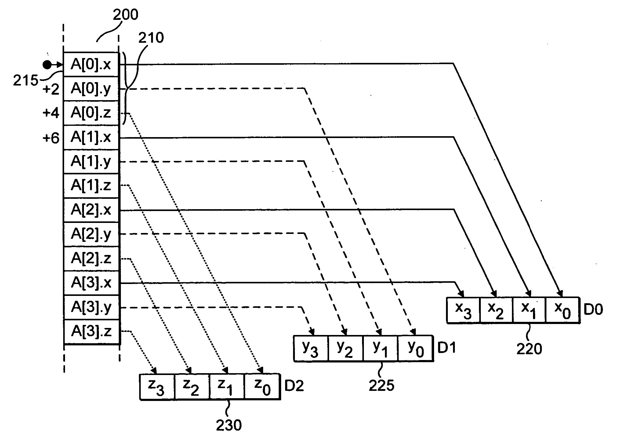
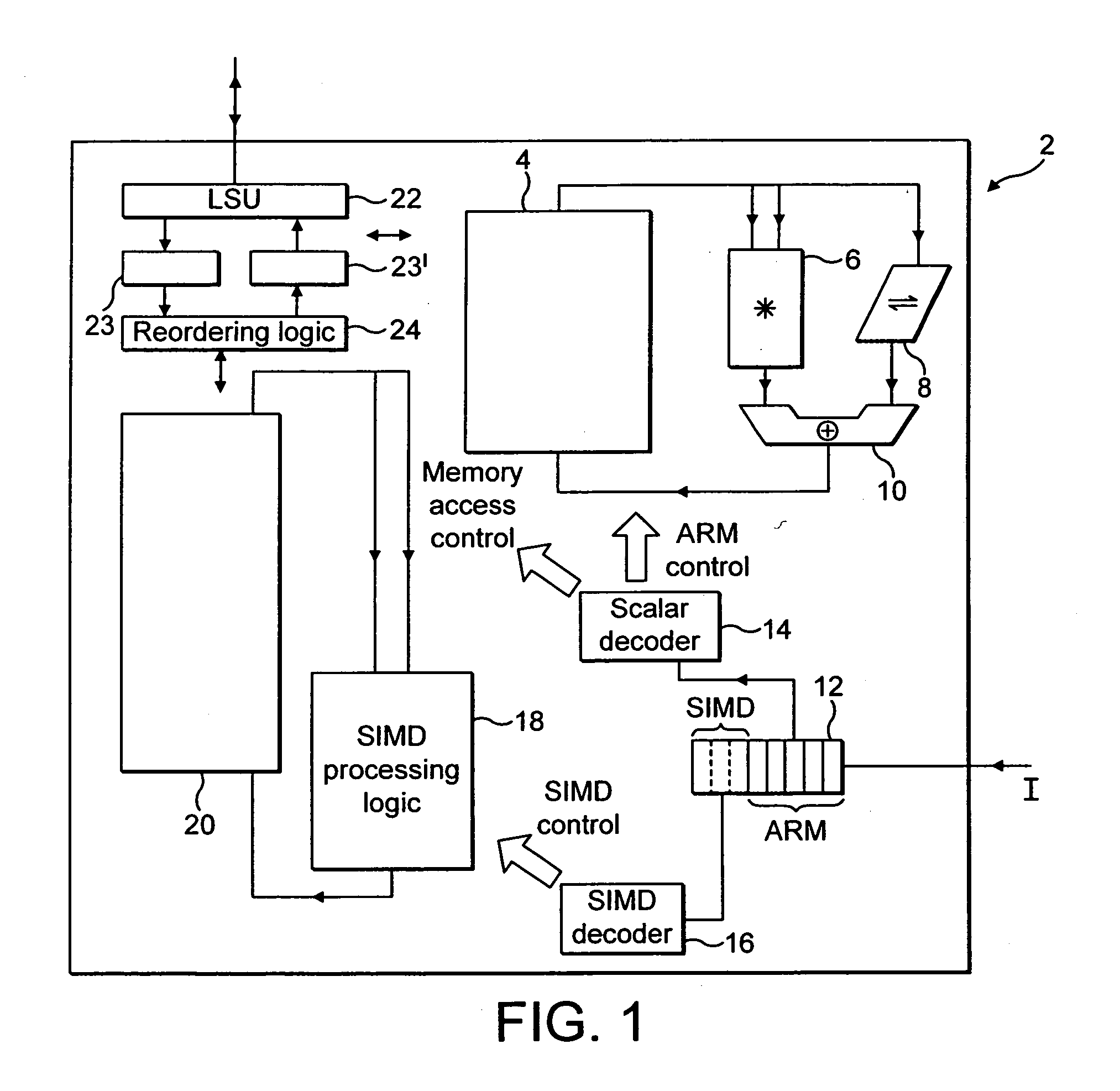
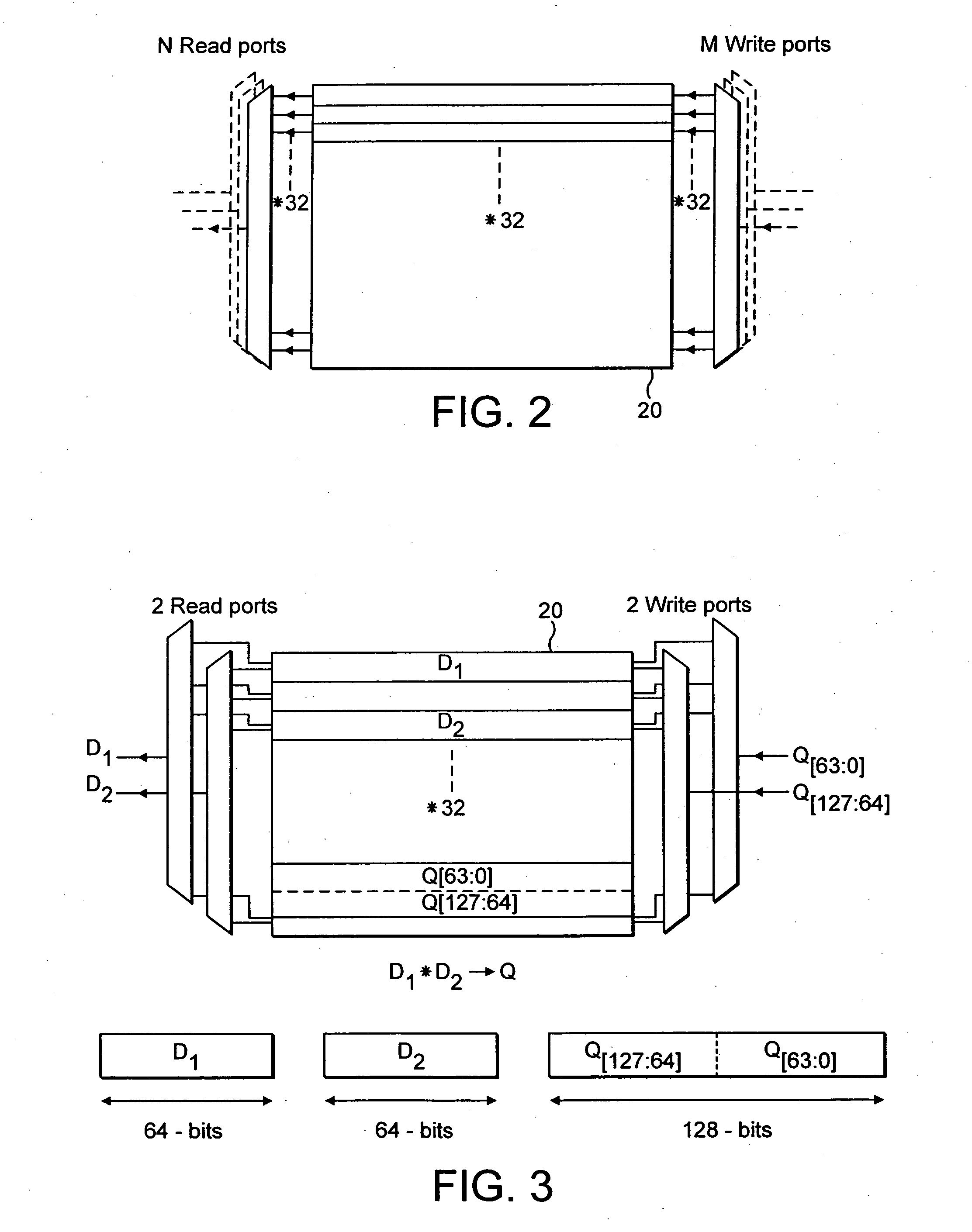
[0090]FIG. 1 schematically illustrates a data processing system (integrated circuit) 2 incorporating both a scalar data processing functionality and a SIMD data processing functionality. The scalar data processing portion can be considered to be a standard ARM processor core incorporating a scalar register data store 4, a multiplier 6, a shifter 8, an adder 10, an instruction pipeline 12 and a scalar decoder 14 as well as many other circuit elements which have not, for the sake of clarity, been illustrated. In operation, such a scalar processor core stores fixed length 32-bit data values within the scalar register data store 4 and manipulates these using the multiplier 6, shifter 8 and adder 10 under control of data processing instructions passed along the instruction pipeline 12 and supplied to the scalar decoder 14. The scalar decoder 14 produces control signals which control the operation of the scalar processing elements in a conventional way.

[0091] As illustrated in FIG. 1 the...


PUM


Abstract

A register data store 20 is provided within a data processing system 2. The register data store 20 may be accessed via registers for which a data processing instruction specifies a register size Q, D and a data element size S16, S8 for the multiple SIMD data elements to be manipulated by that data processing instruction. A given data processing element may be accessed via different registers depending upon the mapping between the register specifier, the register size and the data element size to a particular location within the register data store 20.

Description

BACKGROUND OF THE INVENTION [0001] 1. Field of the Invention [0002] This invention relates to the field of data processing systems. More particularly, this invention relates to data processing systems incorporating a register data store from within which access is made using registers. [0003] 2. Description of the Prior Art [0004] It is known to provide data processing systems, such as ARM processor cores designed by ARM Limited, Cambridge, England, which have a register bank containing a predetermined number of fixed size registers, such as sixteen registers, each being 32 bits in length. A data value stored within such a register may be read from the register by an appropriate read instruction. The instruction writing to that register and the instruction reading from that register will specify the particular register concerned in the same way, e.g. use the same register number / name. [0005] With the increasing demands for data processing systems capable of performing processing ope...

Claims


Application Information

Patent Timeline
Patent Type & Authority Applications(United States)
IPC IPC(8): G06F9/30G06F9/38G06F12/08G06F15/80G06F15/82
CPCG06F9/30036G06F9/30109G06F9/30112G06F9/3887G06F9/30167G06F9/3867G06F9/3885G06F9/30138G06F9/30032G06F9/30098G06F9/30123G06F9/30192G06F9/30105G06F9/30145G06F9/3834G06F15/82G06F12/08G06F9/30G06F15/76
Inventor FORD, SIMONSEAL, DAVID JAMES
Owner ARM LTD
Why Eureka
Try Eureka