Method and apparatus for infilm defect reduction for electrochemical copper deposition

Inactive Publication Date: 2005-08-11
APPLIED MATERIALS INC
View PDF44 Cites 17 Cited by
  • Summary
  • Abstract
  • Description
  • Claims
  • Application Information

AI Technical Summary

Benefits of technology

[0010] Embodiments of the invention generally provide a semiconductor processing apparatus and method configured to minimize voids and cracks in films resulting from rapid anneal temperature ramping. The apparatus of the invention includes a fluid processing cell configured to preheat the substrate prior to the substrate being transferred to the annealing chamber. The fluid processing cell that is used to preheat the substrate is generally an SRD cell. The method of the invention generally includes supplying a heated fluid to an SRD cell on a semiconductor processing pla

Problems solved by technology

However, one challenge with conventional plating systems is that the rapid increase in the temperature of the substrate in the annealing chamber has been shown to cause voids and cracking in the plated layer and between the plated layer and the adjoi

Method used


Image

  • Method and apparatus for infilm defect reduction for electrochemical copper deposition
  • Method and apparatus for infilm defect reduction for electrochemical copper deposition
  • Method and apparatus for infilm defect reduction for electrochemical copper deposition

Examples


Embodiment Construction

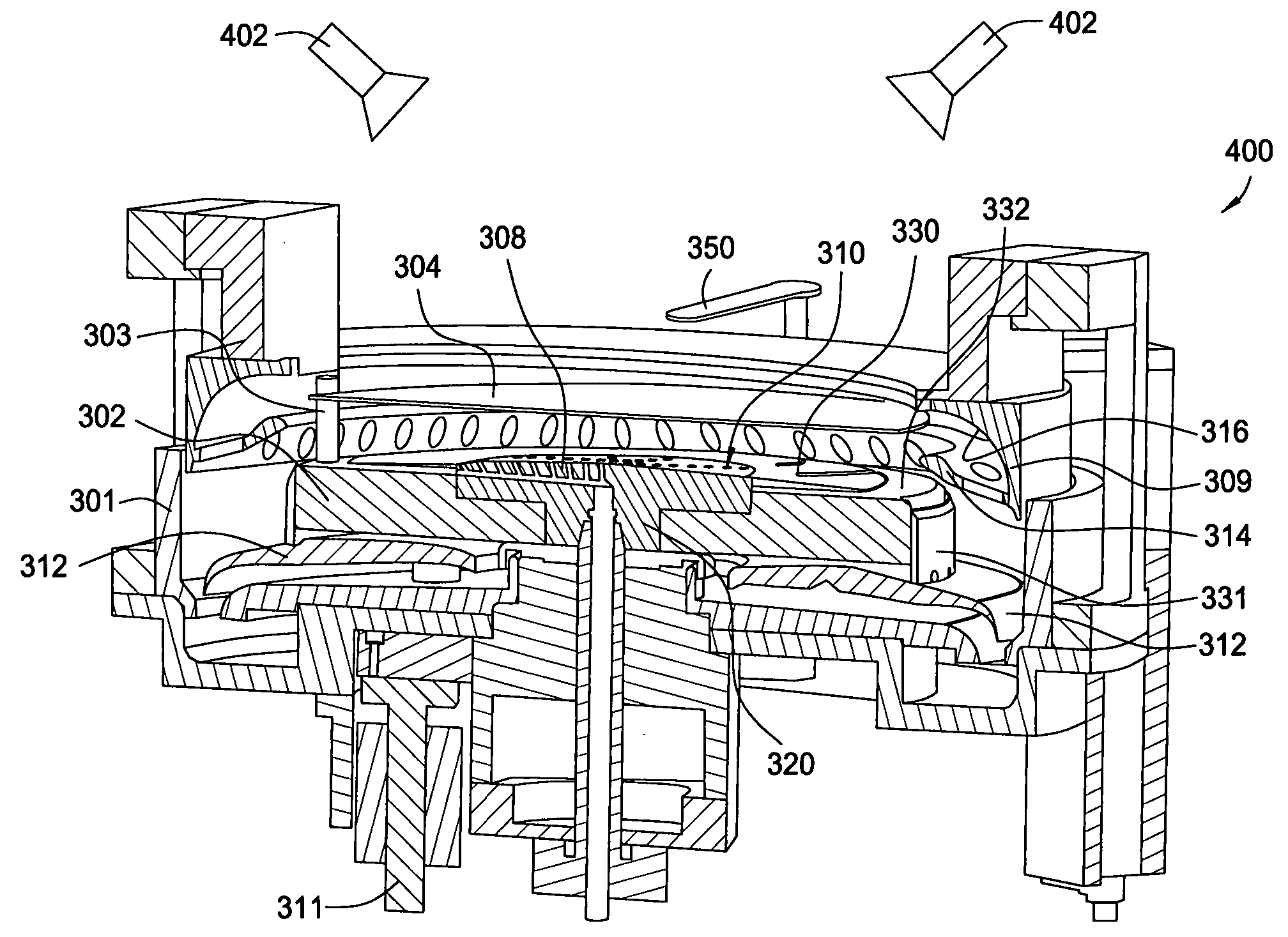
[0019] Embodiments of the invention generally provide an electrochemical plating system configured to plate conductive materials onto semiconductor substrates. The plating system generally includes a substrate loading area in communication with a substrate processing platform. The loading area is generally configured to receive substrate containing cassettes and transfer substrates received from the cassettes into the plating system for processing. The loading area generally includes a robot configured to transfer substrates to and from the cassettes and to the processing platform or a substrate annealing chamber positioned in communication with the loading area. The processing platform generally includes at least one substrate transfer robot and a plurality of substrate processing cells, i.e., ECP cells, bevel clean cells, spin rinse dry cells, substrate cleaning cells, and / or electroless plating cells.

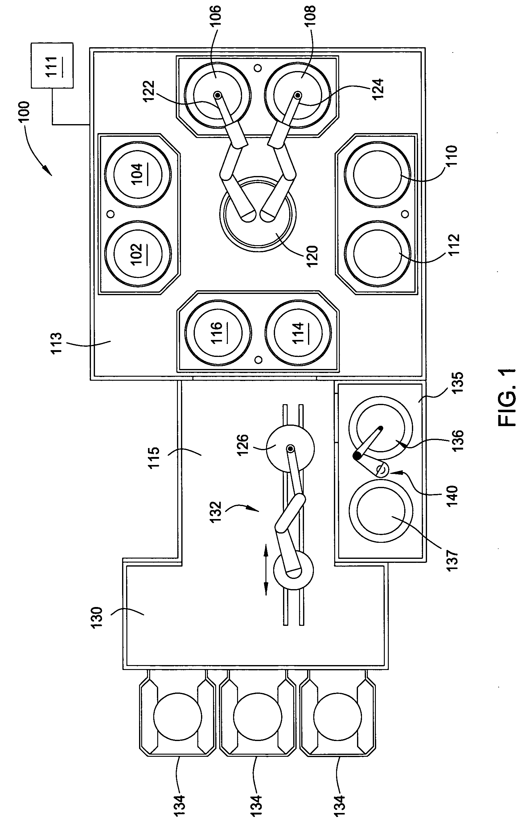
[0020]FIG. 1 illustrates a top plan view of an exemplary ECP system 100 of the ...


PUM

PropertyMeasurementUnit
Temperatureaaaaaaaaaa

Abstract

Embodiments of the invention provide a method and apparatus for processing a substrate. The apparatus includes a substrate rinse cell configured to dispense a heated processing fluid onto the substrate prior to an annealing process. The method includes plating a conductive layer onto a substrate, heating the substrate in a cleaning cell via application of a heated cleaning fluid to the substrate, drying the substrate in the cleaning cell, and annealing the substrate at an annealing station at a temperature of between about 150° C. and about 450° C.

Description

BACKGROUND OF THE INVENTION [0001] 1. Field of the Invention [0002] Embodiments of the invention are generally related to a method for minimizing defects resulting from thermal shock encountered by a substrate during transfer from a fluid processing cell into an annealing chamber. [0003] 2. Description of the Related Art [0004] Metallization of sub-quarter micron sized features is a foundational technology for present and future generations of integrated circuit manufacturing processes. More particularly, in devices such as ultra large scale integration-type devices, i.e., devices having integrated circuits with more than a million logic gates, the multilevel interconnects that lie at the heart of these devices are generally formed by filling high aspect ratio, i.e., greater than about 4:1, interconnect features with a conductive material. The most common conductive material used in large scale integration devices is copper. Copper is generally deposited into the high aspect ratio f...

Claims


Application Information

Patent Timeline
IPC IPC(8): C23C18/16C25D5/50C25D7/12
CPCC23C18/1632C23C18/1694C25D21/08C25D21/02C25D17/001
Inventor HUANG, YI-CHIAU
Owner APPLIED MATERIALS INC
Why Eureka
Try Eureka