Superconductors and methods for making such superconductors

a superconductors and manufacturing method technology, applied in the field of superconductors, can solve the problems of cumbersome and costly processes for the fabrication of such superconductors, and achieve the effects of reducing manufacturing costs, reducing manufacturing costs, and reducing manufacturing costs

Inactive Publication Date: 2005-08-11
MANNHART JOCHEN DIETER +4
View PDF5 Cites 34 Cited by
  • Summary
  • Abstract
  • Description
  • Claims
  • Application Information

AI Technical Summary

Benefits of technology

[0029] Another advantage of the invention is that it simplifies the manufacturing process of superconductors for technical applications by allowing cheaper mass production of polycrystalline high-Tc and other superconductors with large critical current densities. This is the case because the large current densities achieved by the invention relax the requirements on the costly and tedious grain alignment.
[0030] In the following, implementations of the invention shall be described, illustrated by the appended drawings.

Problems solved by technology

At present, the fabrication of such superconductors requires cumbersome and costly processes to optimize the grain boundary alignment.

Method used


Image

  • Superconductors and methods for making such superconductors
  • Superconductors and methods for making such superconductors
  • Superconductors and methods for making such superconductors

Examples


example 1

[0039] In the first embodiment, two YBa2Cu3O7−δ tapes are used which are fabricated by a standard RABiTS Procedure. As substrate a Ni-alloy tape, e.g., Ni—W with a thickness in the range of 20 μm to 100 μm, is employed. According to the standard, published procedures, the tape is rolled and heated, so that a surface texture with aligned grains is produced, although the alignment of the grains is not a critical prerequisite for the invention. The surface orientation of the tape (for Ni, e.g. (111)) has to be chosen to be appropriate for the later growth of a superconductor. On such tapes a buffer layer system is deposited. Such a buffer layer, which itself may consist of various sublayers such as CeO2 / YsZ / CeO2, is deposited on the carrier tape to prevent chemical reactions between the high-Tc film and the carrier tape material, or, e.g, the oxidation of the carrier tape during the growth of the superconductor.

[0040] A variety of materials have been found useful as buffer-layers. Bes...

example 2

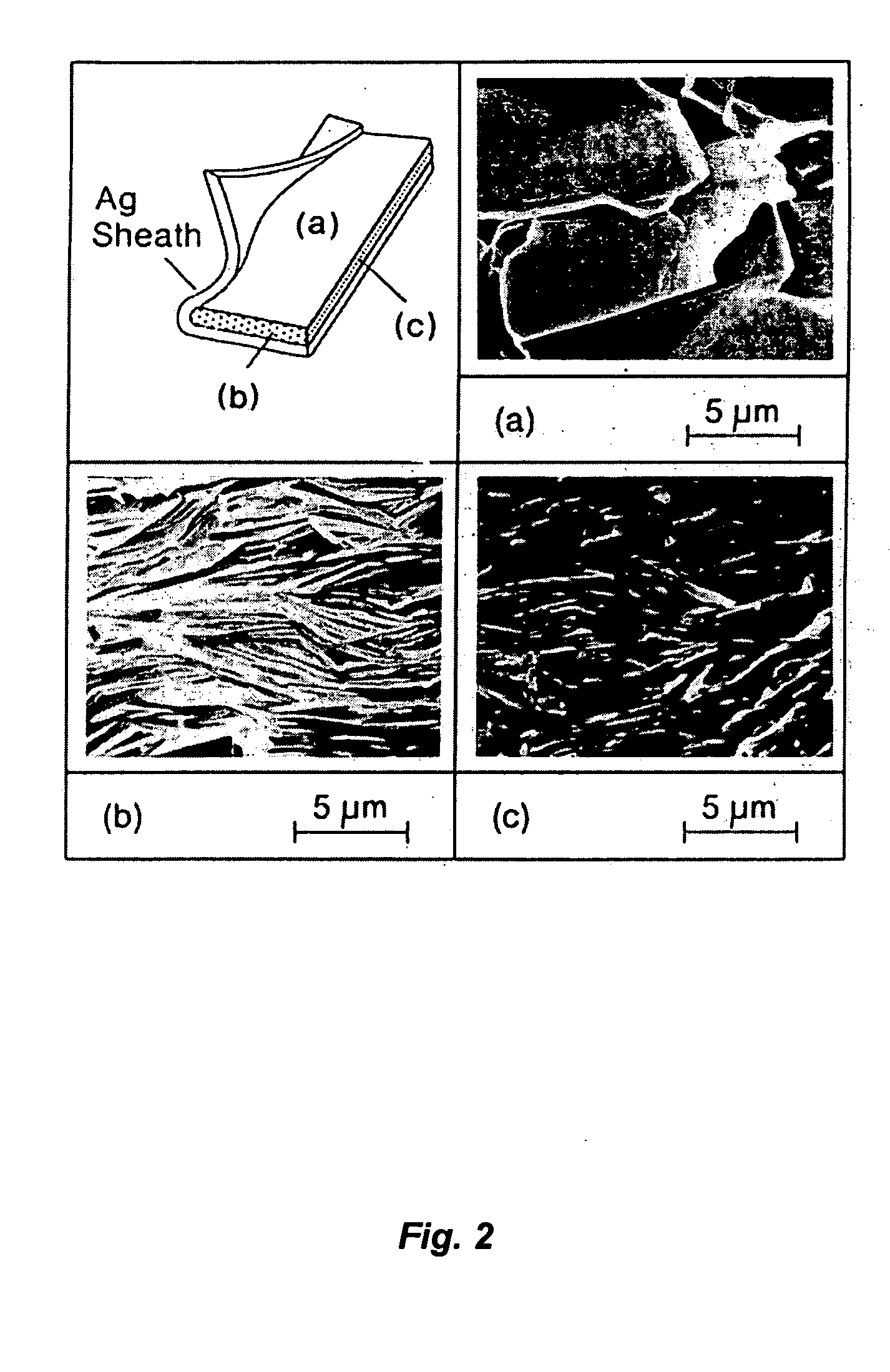
[0043] The second example is again based on coated conductor tapes, fabricated as described in example 1, the difference being that the buffer layers and superconductors are deposited on both sides of the tapes. After the high-Tc superconductor, e.g. YBa2Cu3O7−δ has been deposited, another layer, the intermediate layer, is grown, which is also superconducting, but has a lower melting temperature than YBa2Cu3O7−δ. As revealed by T. Puig et al. in “Self-seeded YBCO welding induced by Ag additives”, Physica C Vol 363, pages 75-79, such a layer may consist, for example, of a 15 wt % Ag+0.7 YBa2Cu3O7−δ O+0.3Y2BaCuO5 composite, the melting temperature of which is about 40° C. lower than that of YBa2Cu3O7−δ. The superconductors are again placed on top of each other and are heated under slight pressure to a temperature of about 990° C. in an appropriate atmosphere (e.g. 0.5 bar of O2), as revealed by T. Puig et al. A superconductor fabricated this way is sketched as illustration in FIG. 6. ...

example 3

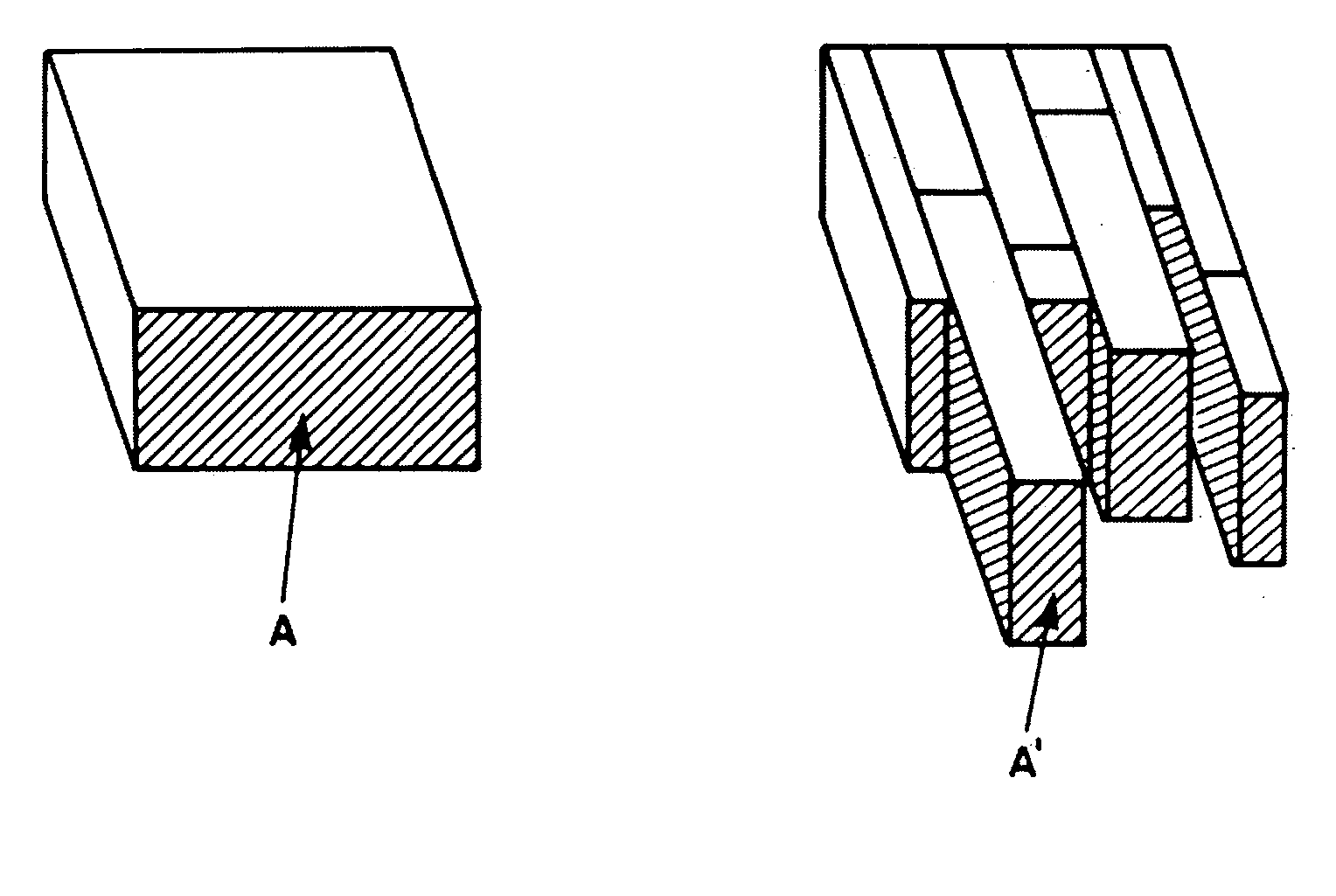
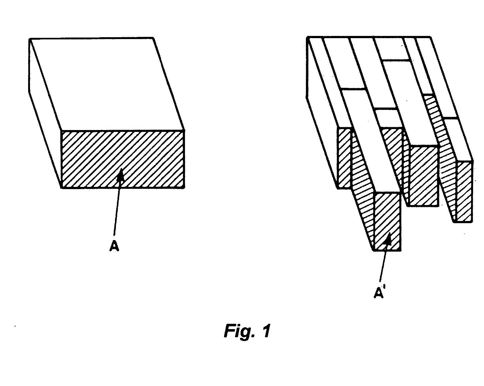
[0044] The superconductor presented as third example is based on a double-sided superconducting tape including a layer with a lower melting temperature than described in example 2. This tape is then rolled up, as sketched in FIG. 7, and welded together like the superconductor in example 2.

[0045] In a modification of this embodiment, a tape covered with a superconducting layer, possibly even on one side only, is folded such that the superconducting layer is folded onto itself and a superconducting contact is established between various areas of one single superconducting layer. This folding step can be repeated several times to obtain a stack of superconducting double-layers.

[0046] It obvious to persons working in the field of superconductivity that, by using the invention, not only tapes for current transport can be fabricated, but that the invention also lends itself for the production of superconductors to be used for other purposes. By using the invention it is readily possible...


PUM

PropertyMeasurementUnit
lengthaaaaaaaaaa
Tc superconductorsaaaaaaaaaa
thicknessaaaaaaaaaa

Abstract

This invention concerns an improvement of the supercurrent carrying capabilities, i.e. the increase of critical current densities, of polycrystalline superconductor structures, especially of high-Tc superconductors fabricated with a coated conductor technique to provide superconducting layers containing flat grains. A superconductor with superior critical current density is obtained by joining, i.e. pressing or otherwise bringing into intensive facial contact, preferably superconducting contact, two or more such superconducting layers.

Description

TECHNICAL FIELD [0001] The present invention relates to superconductors, particularly to the current carrying capabilities of superconductors. It is a proven fact that the critical currents of many superconductors, here polycrystalline superconductors, are limited by grain boundaries formed in them. The invention overcomes this limitation of present superconductors by using alterations for improving the current transport properties of the superconductors' grain boundaries. This is done in principle by optimizing the microstructure of the substrate or of a buffer layer system onto which the superconductor is deposited, such that the polycrystalline superconductor contains large grain boundary areas. BACKGROUND OF THE INVENTION [0002] Based on the new class of superconductors, henceforth referred to as high-Tc superconductors, which were discovered by Bednorz and Müller and disclosed in their article “Possible High-Tc Superconductivity in the Ba—La—Cu—O System”, Zeitschrift für Physik...

Claims


Application Information

Patent Timeline
Patent Type & Authority Applications(United States)
IPC IPC(8): H01L39/14H01L39/24
CPCH01L39/248H01L39/143H10N60/203H10N60/0801
Inventor MANNHART, JOCHEN DIETERHAMMERL, GERMANLEITENMEIER, STEPHANSCHMEHL, ANDREAS FRITZ ALBERTSCHNEIDER, CHRISTOF WALTER
Owner MANNHART JOCHEN DIETER
Why Eureka
Try Eureka