Wire for a display device, a method for manufacturing the same, a thin film transistor array panel including the wire, and a method for manufacturing the same

Inactive Publication Date: 2005-08-11
SAMSUNG DISPLAY CO LTD
View PDF5 Cites 13 Cited by
  • Summary
  • Abstract
  • Description
  • Claims
  • Application Information

AI Technical Summary

Benefits of technology

[0008] An object of the present invention is to provide a wire for a display device a manufacturing method thereof, and a TFT array panel i

Problems solved by technology

However, the wide width of the black matrix established in consideration of the errors in aligning the two panels cause the apertu

Method used


Image

  • Wire for a display device, a method for manufacturing the same, a thin film transistor array panel including the wire, and a method for manufacturing the same
  • Wire for a display device, a method for manufacturing the same, a thin film transistor array panel including the wire, and a method for manufacturing the same
  • Wire for a display device, a method for manufacturing the same, a thin film transistor array panel including the wire, and a method for manufacturing the same

Examples


Example

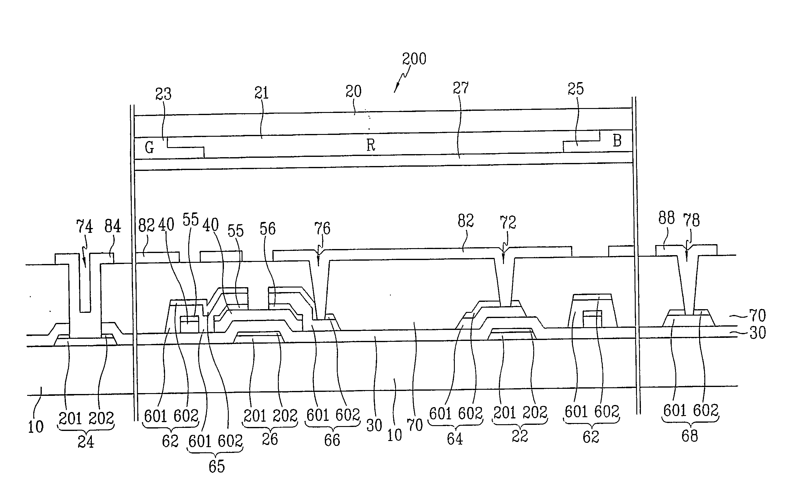
[0053] First, a structure of an LCD according to a first embodiment of the present invention will be described in detail with reference to FIGS. 4 and 5.

[0054]FIG. 4 is a layout view of an LCD according to a first embodiment of the present invention, and FIG. 5 is a sectional view of the LCD shown in FIG. 4 taken along the line IV-IV′.

[0055] Regarding a lower panel 100, a gate wire is formed on a lower insulating substrate 10. The gate wire includes a metal film 201 made of a conductive material having low resistivity such as Cr, Mo, Mo alloy, Al, Al alloy and a metal oxide film 202 preferably made of CrOx, MoOx or oxide of Mo alloy. The gate wire includes a plurality of gate lines 22 extending in a transverse direction, a plurality of gate pads 24 connected to one ends of the gate lines 22 to transmit gate signals from an external device to the gate lines 22, and a plurality of gate electrodes 26 of TFT's connected to the gate lines 22. The gate wire 22, 24 and 26 have a finely-t...

Example

[0082]FIG. 10 is a layout view of a TFT array panel for an LCD according to a second embodiment of the present invention, and FIGS. 11 and 12 are sectional views of the TFT array panel shown in FIGS. 10 taken along the lines XI-XI′ and XII-XII′, respectively.

[0083] A gate wire is formed on an insulating substrate10. Like the first embodiment, the gate wire includes a metal film 201 and a metal oxide film 202. The gate wire includes a plurality of gate lines 22, a plurality of gate pads 24, and a plurality of gate electrodes 26. The gate wire also includes a plurality of storage electrodes 28 parallel to the gate lines 22 on the substrate 10. The storage electrodes 28 are applied with a predetermined voltage such as a common electrode voltage which is inputted to a common electrode of an upper panel from an external device. The storage electrodes 28 overlap storage capacitor conductors 64 connected to pixel electrodes 82 to form storage capacitors for enhancing the charge storing ca...


PUM


Abstract

First, a Cr film and a CrOx film are deposited and patterned using an etchant including 8-12% Ce(NH4)2(NO3)6, 10-20% NH3 and remaining ultra pure water to form a gate wire including a plurality of gate lines, a plurality of gate electrodes and a plurality of gate pads. Next, a gate insulating film, a semiconductor layer and an ohmic contact layer are formed in sequence. A Cr film and CrOx film are deposited in sequence and patterned using an etchant including 8-12% Ce(N114)2(NO3)6, 10-20% NH3 and remaining ultra pure water to form a data wire including a plurality of data lines, a plurality of source electrodes, a plurality of drain electrodes and a plurality of data pads. A passivation layer is deposited and pattered to form a plurality of contact holes respectively exposing the drain electrodes, the gate pads and the data pads. A transparent conductive material or a reflective conductive material is deposited and patterned to form a plurality of pixel electrodes, a plurality of subsidiary gate pads and a plurality of subsidiary data pads electrically connected to the drain electrodes, the gate pads and the data pads, respectively. The gate lines and the data lines with low reflectance are used as a light-blocking film for blocking the light leakage between the pixel areas, and do not increase the black brightness. Accordingly, a separate black matrix need not be provided on the color filter panel, thereby securing both aperture ration of the pixel and high contrast ratio.

Description

BACKGROUND OF THE INVENTION [0001] (a) Field of the Invention [0002] The present invention relates to a wire for a display device and a thin film transistor array panel including the same. [0003] (b) Description of the Related Art [0004] A liquid crystal display (“LCD”) includes an upper panel and a lower panel, and a liquid crystal material interposed therebetween. Such an LCD displays images by applying electric field using electrodes to the liquid crystal material interposed between the two panels and adjusting the strength of the electric field to control the transmittance of light passing through the panels. [0005] One of the panels includes wires transmitting gate signals or image signals, pixel electrodes receiving the image signals, and thin film transistors (“TFTs”) controlling the image signals transmitted to the pixel electrode of each pixel by the gate signals. The other panel includes color filters for implementing a variety of color displays and a black matrix for bloc...

Claims


Application Information

Patent Timeline
IPC IPC(8): G02F1/1343G02F1/1362G02F1/1368G09F9/30H01L21/28H01L21/3205H01L23/52H01L29/417H01L29/423H01L29/49H01L29/786
CPCG02F2001/136295G02F1/136286G02F1/136295
Inventor YU, SEUNG-HEEHONG, MUN-PYORHO, SOO-GUYRHO, NAM-SEOKSONG, KEUN-KYUCHOE, HEE-HWANKIM, BO-SUNGKIM, SANG-GABKANG, SUNG-CHULPARK, HONG-SICK
Owner SAMSUNG DISPLAY CO LTD
Why Eureka
Try Eureka