Thin film transistor array panel and liquid crystal display including the panel

Active Publication Date: 2005-08-11
SAMSUNG DISPLAY CO LTD
View PDF6 Cites 32 Cited by
  • Summary
  • Abstract
  • Description
  • Claims
  • Application Information

AI Technical Summary

Benefits of technology

[0009] In this way, each data line includes a pair of data line branches parallel to each other, the pixel electrodes overlap the data line branches, and a light blocking member covers gaps between the data line brances. Therefore, the parasitic capacitance between the data lines and the pixel electrodes is reduced and the aperture ratio is increased.
[0015] The liquid crystal layer may have several variations. Although the embodiments illustrate TN mode LCDs, the invention can also be employed for a vertical alignment mode. A vertical alignment mode LCD includes a liquid crystal layer having negative dielectric anisotropy and long axes of the liquid crystal molecules are aligned vertical to surfaces of the panels. The vertical alignment mode LCD has cutouts or protrusions provided at the common electrode and the pixel electrodes, which differentiate the tilt directions of the liquid crystal molecules upon the application of electric field to the LC layer, thereby improving so called viewing angle.

Problems solved by technology

However, the overlap of the pixel electrode supplied with a pixel voltage and the data lines transmitting continuously vaying data voltages make parasitice capacitance that may cause several defects.

Method used


Image

  • Thin film transistor array panel and liquid crystal display including the panel
  • Thin film transistor array panel and liquid crystal display including the panel
  • Thin film transistor array panel and liquid crystal display including the panel

Examples


first embodiment

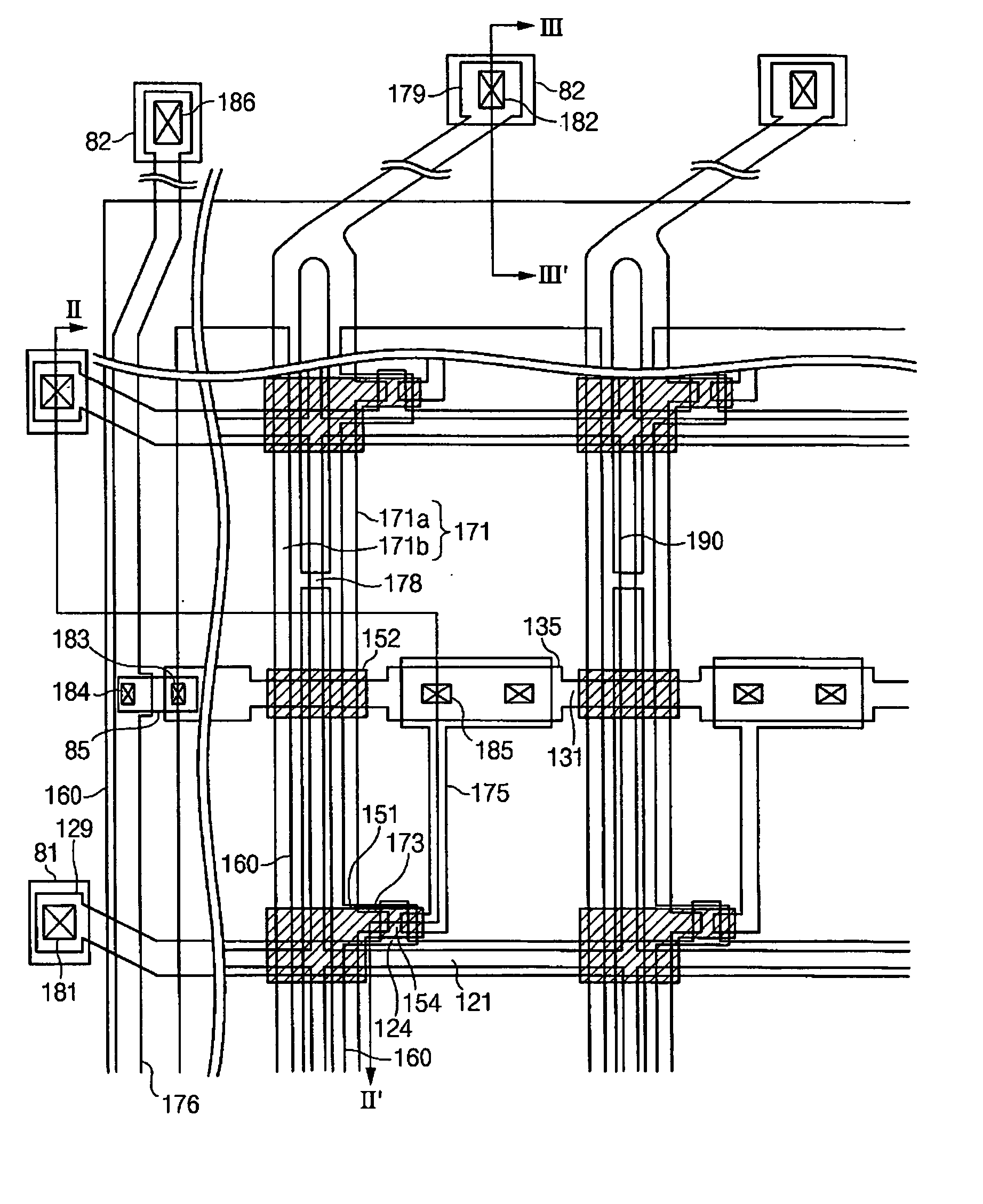
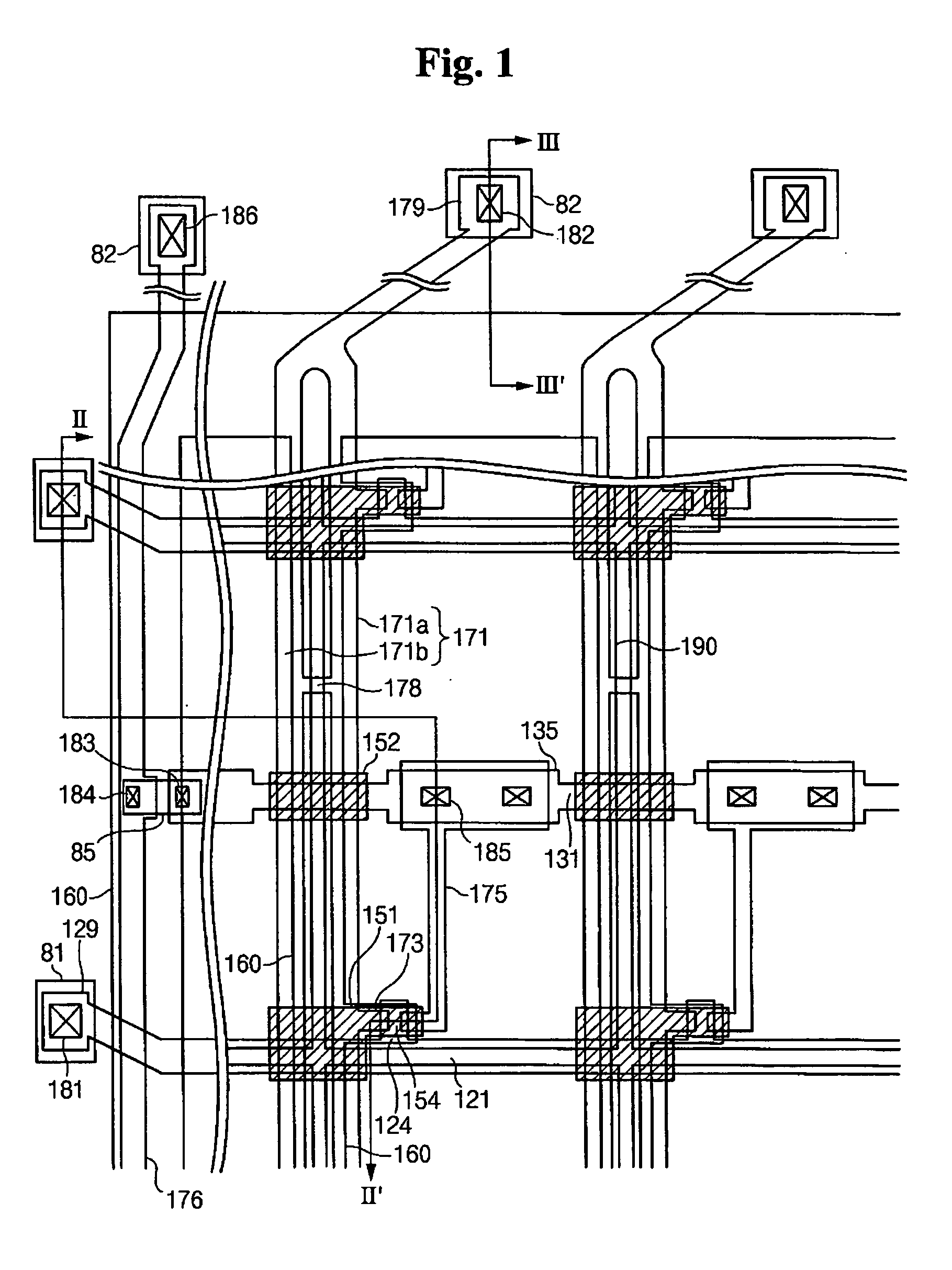
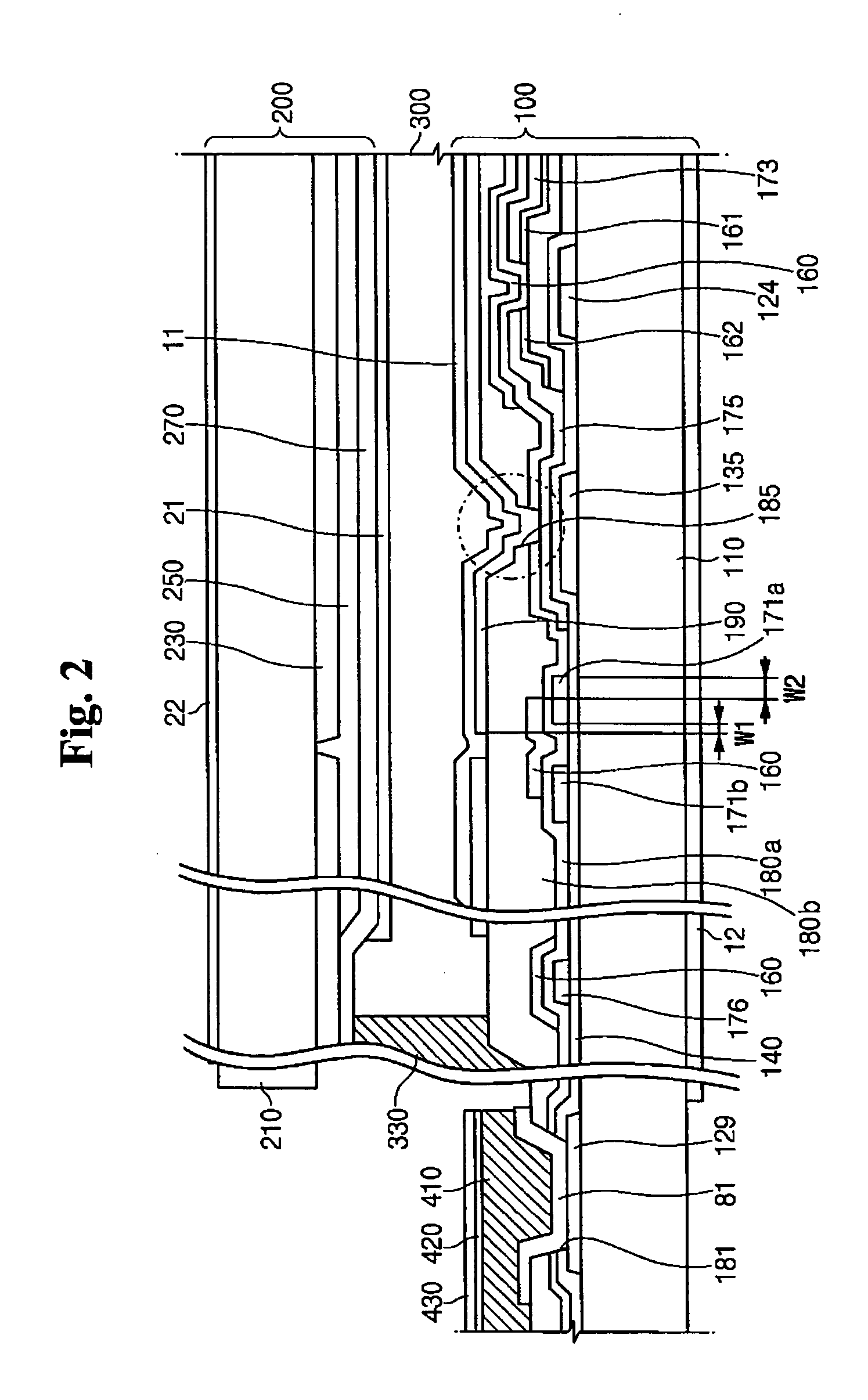
[0036]FIG. 1 is a layout view of a TFT array panel for an LCD according to the present invention, FIG. 2 is a sectional view of an LCD including the TFT array panel shown in FIG. 1 and a common electrode panel taken along the line II-II′, and FIG. 3 is a sectional view of an LCD including the TFT array panel shown in FIG. 1 and a common electrode panel taken along the line III-III′.

[0037] Referring to FIGS. 2 and 3, an LCD according to this embodiment includes a TFT array panel 100 and the common electrode panel 200 facing each other and an LC layer 300 and a sealant 330. On the TFT array panel 100, a film 430 such as a flexible printed circuit film having signal lines 420 and an anisotropic conductive film 410 attaching the film 430 to the panel 100 are formed.

[0038] First, the TFT array panel 100 is schematically described.

[0039] Referring to FIG. 1, a plurality of pixel electrodes 190 preferably made of transparent conductive material such as indium tin oxide (ITO) or indium zi...

second embodiment

[0077] Referring to FIG. 4-6, an LCD according to the present invention will be described in detail.

[0078]FIG. 4 is a layout view of a TFT array panel for an LCD according to a second embodiment of the present invention, FIG. 5 is a sectional view of an LCD including the TFT array panel shown in FIG. 4 and a common electrode panel taken along the line V-V′, and FIG. 6 is a sectional view of an LCD including the TFT array panel shown in FIG. 4 and a common electrode panel taken along the line VI-VI′.

[0079] The LCD according to the second embodiment has a layout and a structure similar to the LCD according to the first embodiment.

[0080] Regarding the TFT array panel 100, a plurality of gate lines 121 including gate electrodes 124 and a plurality of storage electrode lines 131 are formed on a substrate 110, and a gate insulating layer 140, a plurality of semiconductor islands 154, and a plurality of ohmic contact islands 161 and 162 are sequentially formed thereon. A plurality of dat...

third embodiment

[0084] Referring to FIG. 7-9, an LCD according to the present invention will be described in detail.

[0085]FIG. 7 is a layout view of a TFT array panel for an LCD according to a second embodiment of the present invention, FIG. 8 is a sectional view of an LCD including the TFT array panel shown in FIG. 7 and a common electrode panel taken along the line VII-VII′, and FIG. 9 is a sectional view of an LCD including the TFT array panel shown in FIG. 7 and a common electrode panel taken along the line IX-IX′.

[0086] The LCD shown in FIG. 7-9 has a layout and a structure similar to the LCD shown in FIG. 4-6.

[0087] Regarding the TFT array panel 100, a plurality of gate lines 121 including gate electrodes 124 and a plurality of storage electrode lines 131 are formed on a substrate 110, and a gate insulating layer 140, a plurality of semiconductor islands 154, and a plurality of ohmic contact islands 161 and 162 are sequentially formed thereon. A plurality of data lines 171 including source ...


PUM

PropertyMeasurementUnit
anglesaaaaaaaaaa
inclination angleaaaaaaaaaa
distance w2aaaaaaaaaa

Abstract

A thin film transistor (TFT) array panel is provided, which includes: a plurality of gate lines transmitting gate signals; a plurality of data lines intersecting the gate lines and transmitting data signals, each data line including first and second data line branches electrically connected to each other and spaced apart from each other; a plurality of pixel electrodes electrically connected to the gate lines and the data lines through thin film transistor and covering edges of the first or the second data line branches; a passivation layer disposed between the data lines and the pixel electrodes; and a light blocking member covering gaps between the first data line branches and the second data line branches.

Description

BACKGROUND OF THE INVENTION [0001] (a) Field of the Invention [0002] The present invention relates to a thin film transistor array panel and a liquid crystal display including the panel having high aperture ratio. [0003] (b) Description of Related Art [0004] A liquid crystal display (LCD) generally includes an upper panel provided with a common electrode, a lower panel having thin film transistors (TFTs) and pixel electrodes, and a liquid crystal (LC) layer interposed between the panels. The pixel electrodes and the common electrode are supplied with different voltages to generate electric field that changes orientations of LC molecules, thereby adjusting light transmittance to display images. [0005] One of important issues of the LCD is an aperture ratio and high aperture ratio increases the luminance of the LCD and following several advantages. For this purpose, a pixel electrode and data lines adjacent therto overlap each other. However, the overlap of the pixel electrode supplie...

Claims


Application Information

Patent Timeline
Patent Type & Authority Applications(United States)
IPC IPC(8): G02F1/1333G02F1/133G02F1/136G02F1/1362G02F1/1368G02F1/139H01L21/28H01L21/3205H01L23/52H01L29/417H01L29/423H01L29/49H01L29/786
CPCG02F1/136209G02F1/136286G02F2201/40G02F2001/136222G02F1/1393G02F1/136222
Inventor KIM, DONG-GYUKIM, SANG-SOO
Owner SAMSUNG DISPLAY CO LTD
Why Eureka
Try Eureka