Method for energy-assisted atomic layer deposition and removal

a technology of atomic layer deposition and removal, applied in the field of semiconductors, can solve the problems of limiting the useful range of gate oxides to about 1.8 nm, reducing the useful range of gate oxides, and prior art fabrication techniques such as chemical vapor deposition (cvd) are increasingly incapable of meeting the requirements of forming advanced thin films, and achieves the effect of high energy and facilitates the reaction of the first reactant gas

Inactive Publication Date: 2005-08-11
HELMS JR AUBREY L +3
View PDF32 Cites 347 Cited by
  • Summary
  • Abstract
  • Description
  • Claims
  • Application Information

AI Technical Summary

Benefits of technology

[0007] In one aspect of the invention, there is provided a method of energy-assisted atomic layer deposition of a film on a substrate. According to the EALD method of the invention, a substrate is placed in a reaction chamber suitable for carrying out the method. Optionally, the substrate may first be pre-treated to condition the surface of the substrate. A first gaseous precursor is introduced into the reactor about the substrate. Energy assistance is provided by exposing the gas and substrate to first pulse of electromagnetic irradiation such that radical species from the gas are formed. Examples of suitable electromagnetic radiation include, but are not limited to, visible light radiation, infrared radiation, ultraviolet radiation, microwave radiation, radio frequency radiation, and the like. In another embodiment, radiation with high energy such as “vacuum ultraviolet (VUV) radiation” is employed to initiate the desired chemical reactions at or near room temperature. It will be clear to one of ordinary skill in the art that the amount of energy of the electromagnetic radiation is selected using routine experimentation so as to most advantageously initiate the desired reaction. The radiation may be supplied in a coherent form from a device such as a laser, or in a non-coherent (i.e. out of phase) form from a device such as a lamp.
[0008] The use of electromagnetic radiation facilitates the reaction of the first reactant gas with the stable surface. The radical species react with the surface to terminate the surface with the radical species. The excess first gaseous precursor and radical species are removed from the reaction chamber by evacuating with a vacuum pump, pu

Problems solved by technology

As oxide films are scaled down, the tunneling leakage current becomes significant and limits the useful range for gate oxides to about 1.8 nm or more.
However, prior art fabrication techniques such as chemical vapor deposition (CVD) are increasingly unable to meet the requirements of forming these advanced thin films.
While CVD processes can be tailored to provide conformal films with improved step coverage, CVD processes often require high processing temperatures, result in incorporation of high impurity concentrations, and have poor precursor or reactant utilization efficienc

Method used


Image

  • Method for energy-assisted atomic layer deposition and removal
  • Method for energy-assisted atomic layer deposition and removal
  • Method for energy-assisted atomic layer deposition and removal

Examples


Embodiment Construction

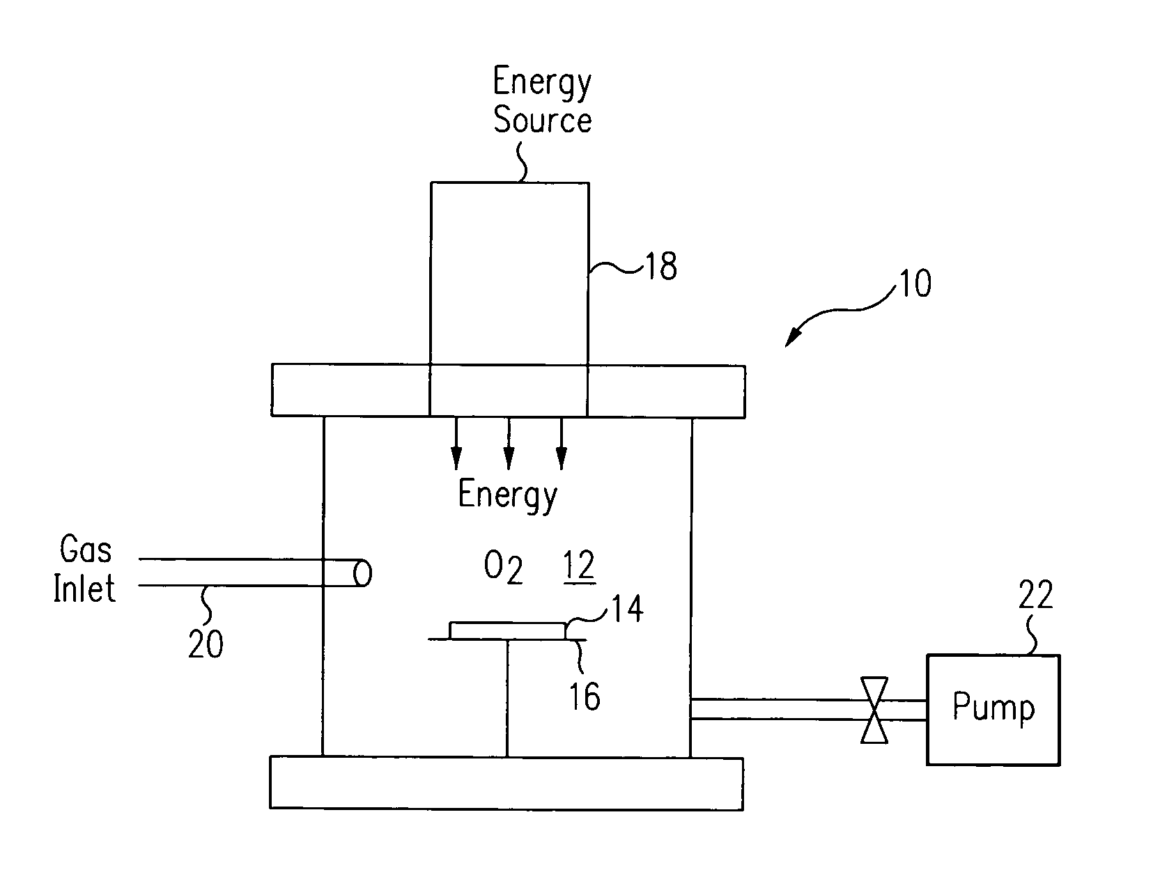
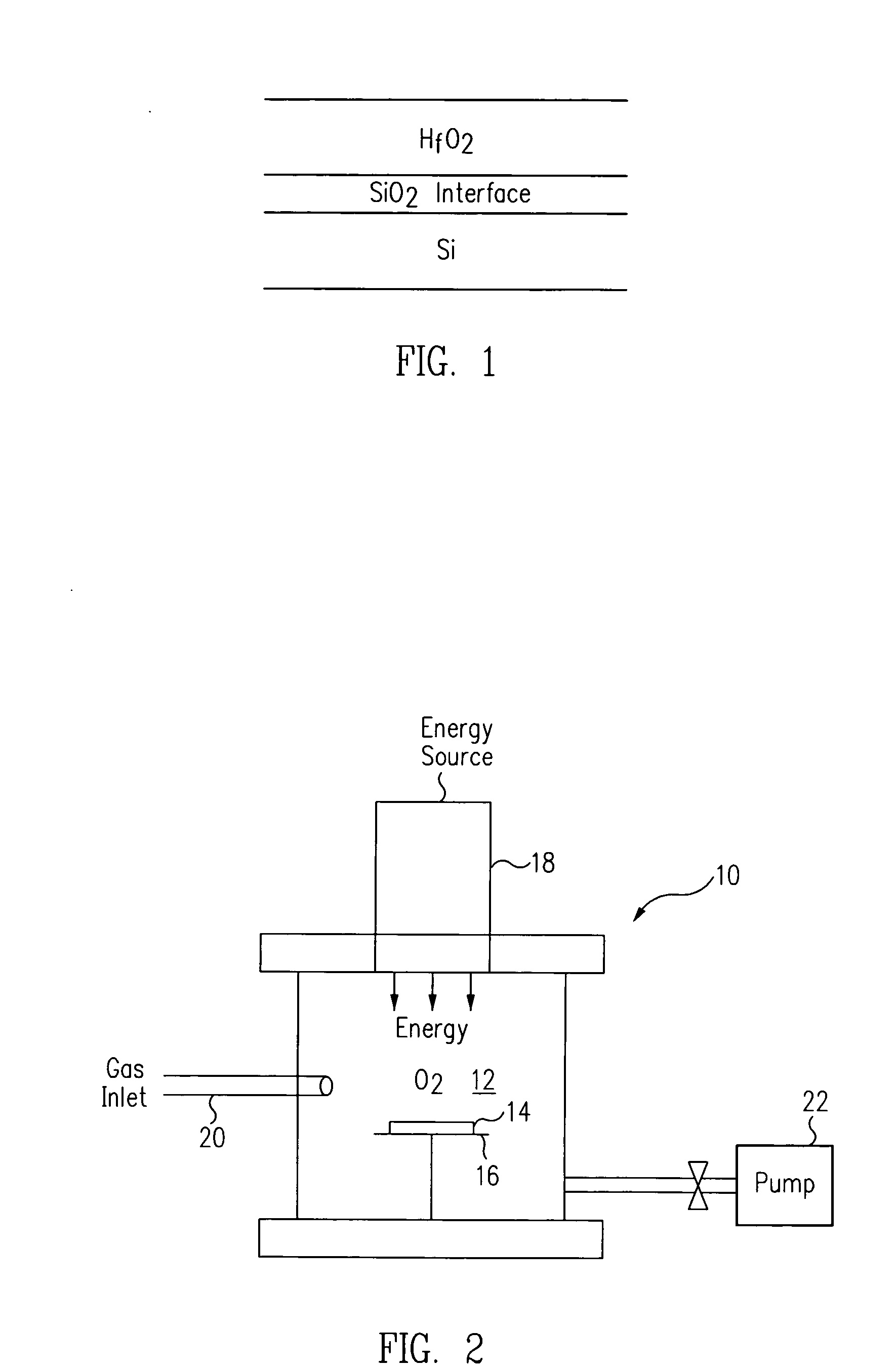
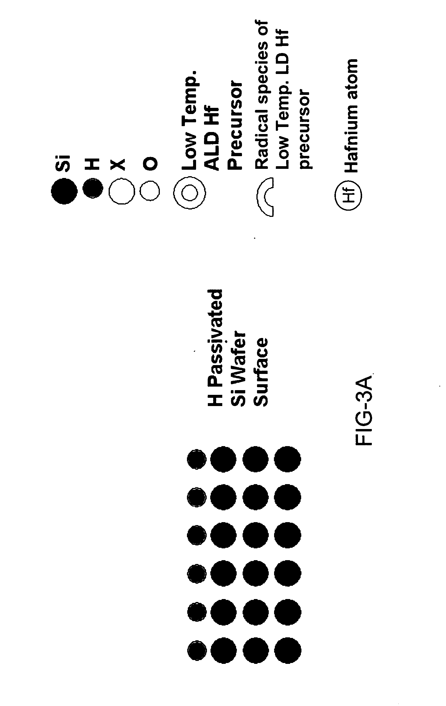
[0014] In general, the present invention provides a method and system of forming films on semiconductor devices and wafers by energy-assisted atomic layer deposition and removal. More specifically, in one embodiment of the present invention, a method of atomic layer deposition of a film on a substrate is provided. In general, the method of the present invention is comprised of the following steps: a substrate is placed in a reaction chamber. The substrate may be a bare silicon substrate, or alternatively may have a film deposited on the surface of the substrate. Optionally, the substrate may be pre-treated to condition the surface of the substrate. Pre-treatment may be employed to clean and / or activate the surface of the substrate.

[0015] A first gaseous precursor is introduced into the reaction chamber about the surface of the substrate. To initiate a desired chemical reaction with the film on the surface of the substrate, energy is employed. Specifically, the gaseous precursor and...


PUM

PropertyMeasurementUnit
Temperatureaaaaaaaaaa

Abstract

A method for energy-assisted atomic layer deposition and removal of a dielectric film are provided. In one embodiment a substrate is placed into a reaction chamber and a gaseous precursor is introduced into the reaction chamber. Energy is provide by a pulse of electromagnetic radiation which forms radical species of the gaseous precursor. The radical species react with the surface of the substrate to form a radical terminated surface on the substrate. The reaction chamber is purged and a second gaseous precursor is introduced. A second electromagnetic radiation pulse is initiated and forms second radical species. The second radical species of the second gas react with the surface to form a film on the substrate. Alternately, the gaseous species can be chosen to produce radicals that result in the removal of material from the surface of the substrate.

Description

RELATED APPLICATIONS [0001] This application claims priority to and the benefit of U.S. Provisional Application Ser. No. 60 / 391,012, filed on Jun. 23, 2002 and U.S. Provisional Application Ser. No. 60 / 396,743, filed on Jul. 19, 2002, the disclosures of both are hereby incorporated by reference in its entirety.FIELD OF THE INVENTION [0002] The present invention relates generally to the field of semiconductors. More specifically, the present invention relates to energy-assisted atomic layer deposition and removal of films on semiconductor devices and wafers. BACKGROUND OF THE INVENTION [0003] Semiconductor devices of future generation require thin dielectric films for metal oxide silicon (MOS) transistor gates, and capacitor dielectrics. As oxide films are scaled down, the tunneling leakage current becomes significant and limits the useful range for gate oxides to about 1.8 nm or more. [0004] High dielectric constant (“high-k”) metal oxides have been considered as possible alternative...

Claims


Application Information

Patent Timeline
IPC IPC(8): C23C16/44C23C16/455H01L21/302C23C16/48H01L21/314H01L21/316
CPCC23C16/45536C23C16/45542H01L21/31645H01L21/3141C23C16/482H01L21/02301H01L21/0228H01L21/02189H01L21/02277H01L21/02205H01L21/02181
Inventor HELMS JR, AUBREY LKAPKIN, KEREMLEE, SANG-INSENZAKI, YOSHIHIDE
Owner HELMS JR AUBREY L
Why Eureka
Try Eureka