Wafer-level chip scale package and method for fabricating and using the same

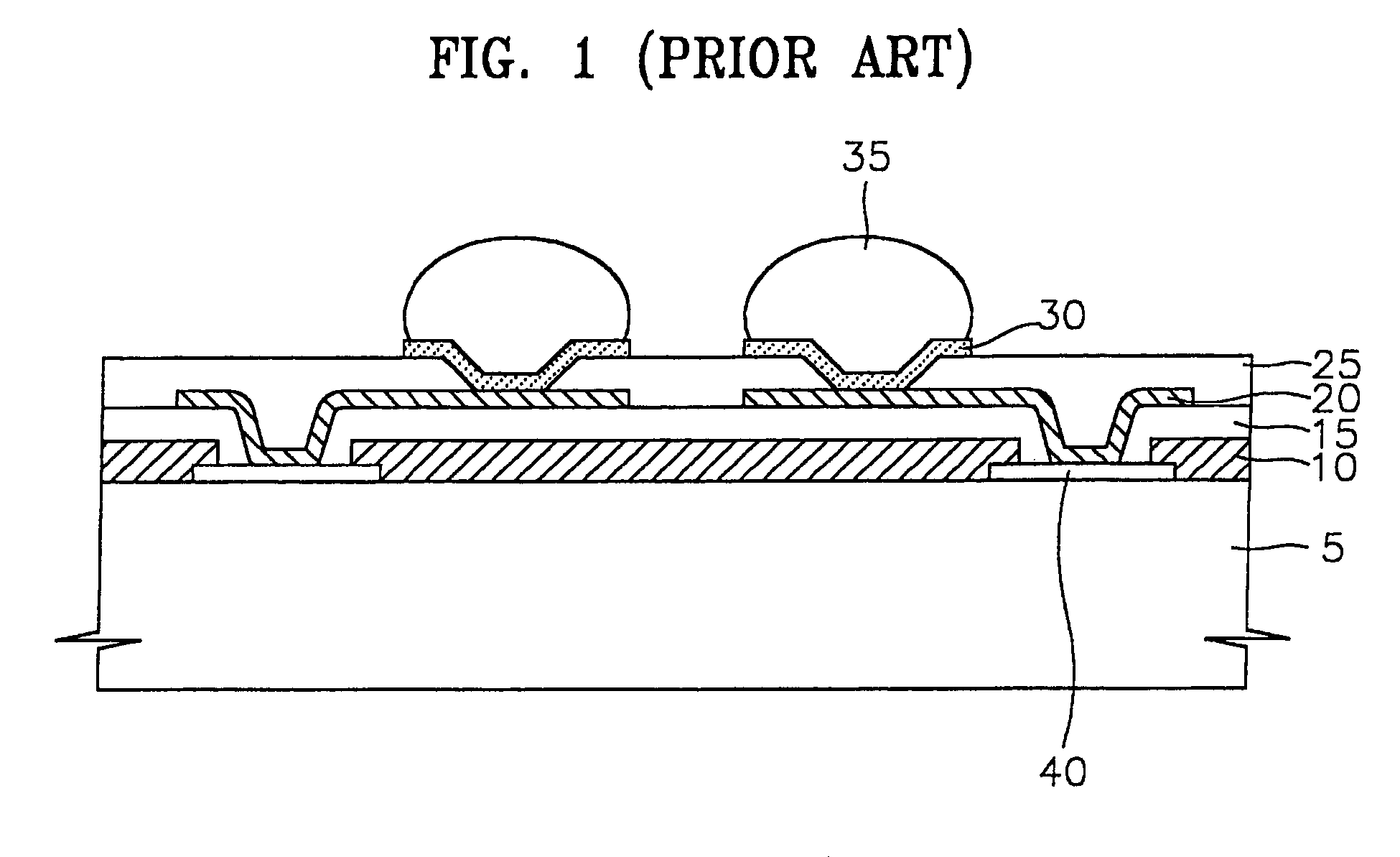
a technology of wafer-level chips and scales, which is applied in the direction of semiconductor devices, semiconductor/solid-state device details, electrical apparatus, etc., can solve the problems of short circuits, cracks and deformations of pattern b>20/b>, and penetrate the solder connection, so as to reduce manufacturing costs

Inactive Publication Date: 2005-08-11
SEMICON COMPONENTS IND LLC
View PDF28 Cites 93 Cited by
  • Summary
  • Abstract
  • Description
  • Claims
  • Application Information

AI Technical Summary

Benefits of technology

[0010] The invention provides a packaged semiconductor device (a wafer-level chip scale package) containing no UBM between a chip pad and an RDL pattern. As well, the device contains only a single non-polymeric insulation layer between the RDL pattern and the sold

Problems solved by technology

In these areas, short circuits can occur and the pattern 20 can crack and deform in these areas due to stresses.
Thus, there is a higher possibility that moisture penetrates into the solder connection 52 and decreases the reliability of the solder connection 52.
Fourth, the package 50 is completed only by carrying out many processing steps and, therefore, manufactu

Method used


Image

  • Wafer-level chip scale package and method for fabricating and using the same
  • Wafer-level chip scale package and method for fabricating and using the same
  • Wafer-level chip scale package and method for fabricating and using the same

Examples


Embodiment Construction

[0027] The invention will now be described more fully with reference to the accompanying drawings, in which one aspect of the invention is shown. This invention may, however, be embodied in many different forms and should not be construed as being limited to the aspects set forth herein. Rather, these aspects are provided so that this disclosure will be thorough and complete and will fully convey the concept of the invention to those skilled in the art. Although the invention is described with respect to IC chips, the invention could be used for other devices where packaging is needed, i.e., silicon MEMS devices.

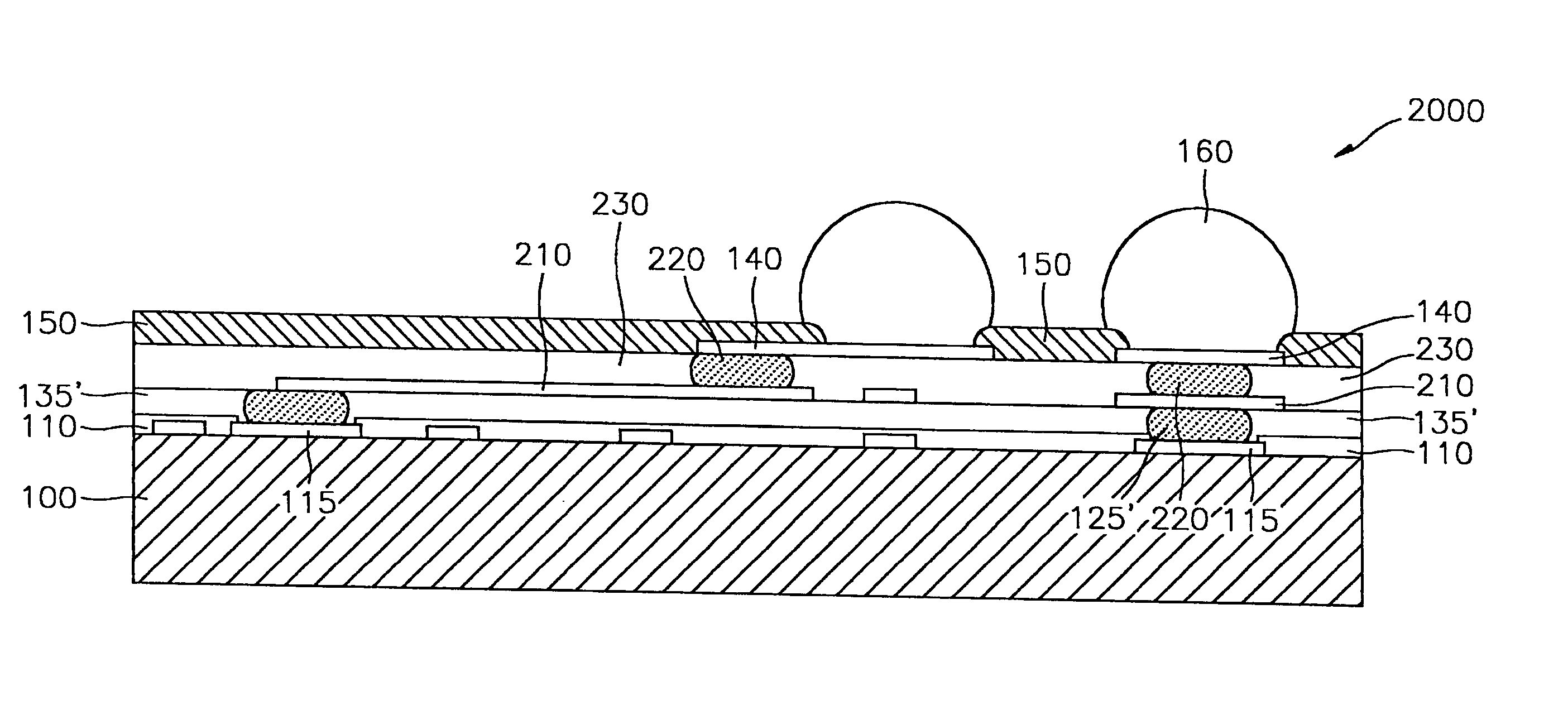
[0028]FIGS. 4 through 10 illustrate one aspect of the invention for fabricating a wafer-level chip scale package containing a re-distributed line (RDL) pattern that is not inclined between the bottom of a solder bump and the top surface of a chip pad. Referring to FIG. 4, a substrate 100 is prepared on which a passivation layer 110 and a chip pad 115 are formed. The substra...


PUM


Abstract

A packaged semiconductor device (a wafer-level chip scale package) containing no UBM between a chip pad and an RDL pattern is described. As well, the device contains only a single non-polymeric insulation layer between the RDL pattern and the solder bump. The single non-polymeric insulation layer does not need high temperature curing processes and so does not induce thermal stresses into the device. As well, manufacturing costs are diminished by eliminating the UBM between the chip pad and the RDL pattern.

Description

REFERENCE TO RELATED APPLICATIONS [0001] This application is a continuation-in-part of U.S. patent application Ser. No. 10 / 295,281, the entire disclosure of which is incorporated herein by reference.FIELD OF THE INVENTION [0002] The invention generally relates to methods for fabricating integrated circuits (ICs) and semiconductor devices and the resulting structures. Specifically, the invention relates to a semiconductor package and a method for fabricating and using the same. More particularly, the invention relates to a wafer level chip scale package and a method for fabricating and using the same. BACKGROUND OF THE INVENTION [0003] Recent advancements in the electronics industry, especially with personal computers (PC), mobile phones, and personal data assistants (PDA), have triggered a need for light, compact, and multi-functional power systems that can process large amounts of data quickly. These advancements have also triggered a reduction in the size of semiconductor chips an...

Claims


Application Information

Patent Timeline
IPC IPC(8): H01L23/31H01L23/485
CPCH01L23/3114H01L24/10H01L24/13H01L2224/0231H01L2224/13099H01L2924/01013H01L2924/01022H01L2924/01029H01L2924/01046H01L2924/01075H01L2924/01078H01L2924/01079H01L2924/14H01L2924/01024H01L2924/01033H01L2924/01047H01L2924/014H01L2224/0401H01L2924/00H01L24/02H01L24/03H01L24/05H01L24/11H01L24/94H01L2224/02333H01L2224/0384H01L2224/05548H01L2224/05624H01L2224/05647H01L2224/05655H01L2224/05666H01L2224/05671H01L2224/0615H01L2224/13H01L2224/13024H01L2924/0001H01L2924/351H01L2924/00014H01L2224/02H01L2924/01023H01L2924/013
Inventor JOSHI, RAJEEVWU, CHUNG- LINLEE, SANG-DOCHOI, YOON-HWA
Owner SEMICON COMPONENTS IND LLC
Why Eureka
Try Eureka