Dynamic command and/or address mirroring system and method for memory modules

a memory module and dynamic command technology, applied in the field of memory modules, can solve the problems of excessive cross-talk between conductors, difficult routing of conductors to externally accessible terminals of memory devices, and relatively high cost of providing substrates

Inactive Publication Date: 2005-08-11
ROUND ROCK RES LLC
View PDF99 Cites 94 Cited by
  • Summary
  • Abstract
  • Description
  • Claims
  • Application Information

AI Technical Summary

Benefits of technology

[0014] A memory module according to one aspect of the invention includes an insulative substrate; on which a plurality of identical memory devices mounted on first and second opposed surfaces of the insulative substrate. The memory devices are mounted on the substrate in a mirrored configuration. As a result, a plurality of terminals of each of the memory devices mounted on the first surface are interconnected to respective, correspondingly positioned terminals of a respective one of the memory devices mounted on the second surface. Address and command signals are coupled to the interconnected terminals. Significantly, either the address signals, the command signals or both the address and command signals are coupled to the i

Problems solved by technology

The decreased spacing between memory devices and the increased number of terminals has made it more difficult to route conductors to the externally accessible terminals of the memory devices.
However, it is relatively expensive to provide substrates having a large number of layers, and a large number of closely spaced layers can result in excessive cross-talk between conductors on different layers and excessive conductor capacitance.
The two different packages can theoretically use the same integrated circuit chip, but, in practice, this is not always feasible.
Not only is it sometimes difficult to route signal lines from a circuit node to either of two different terminals, doing so creates an undesirable stub connection to the signal path between the terminal and the circuit node.
This stub connection can produce signal reflections that can degrade the performance of the integrated circuit.
The need to develop and stock two different integrated circuit packages, even if the same chip can be used for both packages, can significantly increase the cost of mirro

Method used


Image

  • Dynamic command and/or address mirroring system and method for memory modules
  • Dynamic command and/or address mirroring system and method for memory modules
  • Dynamic command and/or address mirroring system and method for memory modules

Examples


Embodiment Construction

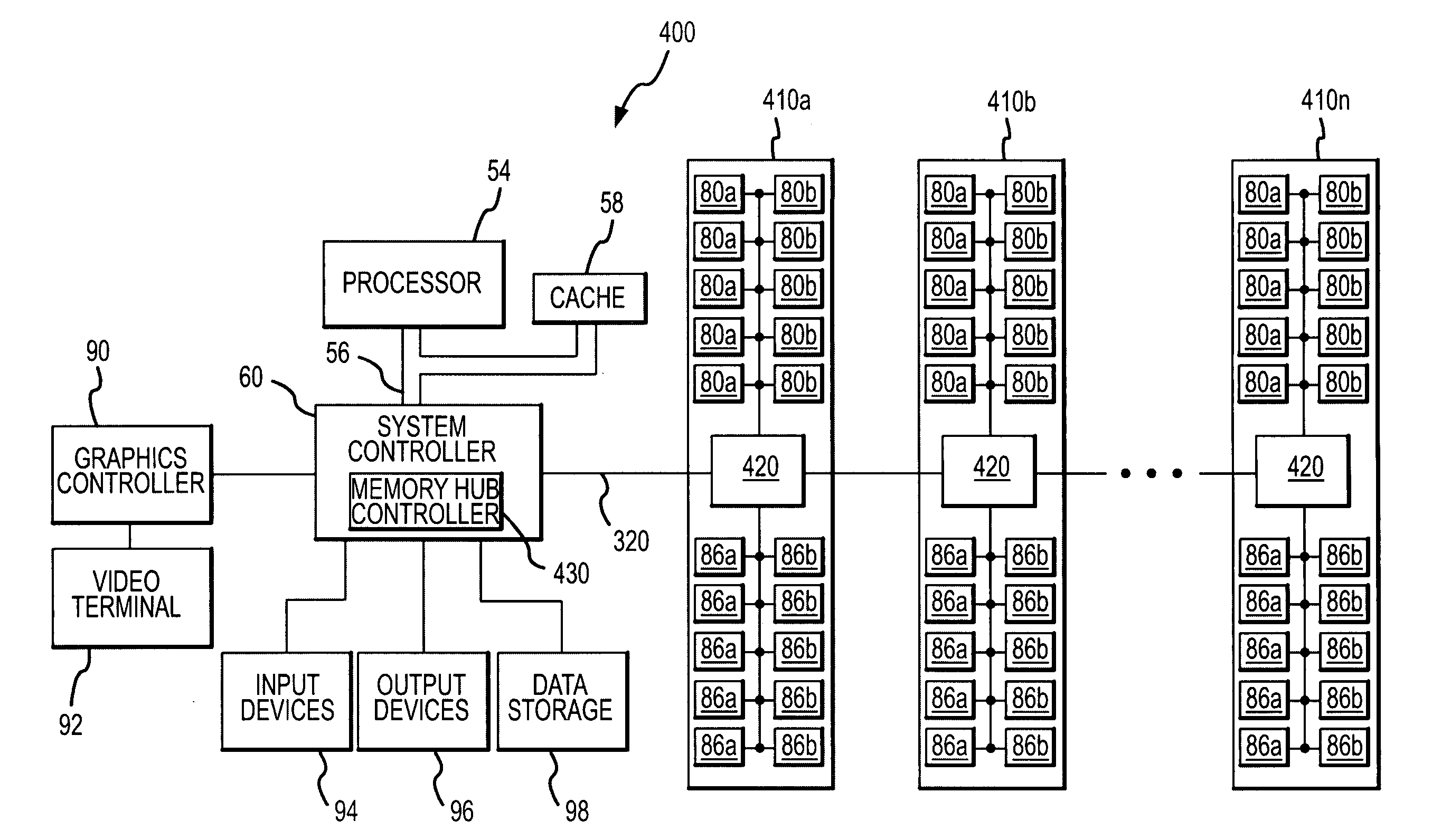
[0022] A computer system 50 according to one embodiment of the invention is shown in FIG. 4. The computer system 50 includes a processor 54 for performing various computing functions, such as executing specific software to perform specific calculations or tasks. The processor 54 includes a processor bus 56 that normally includes an address bus, a control bus, and a data bus. The processor bus 56 is typically coupled to a cache memory 58, which, is typically static random access memory (“SRAM”) device. Finally, the processor bus 56 is coupled to a system controller 60, which is also sometimes referred to as a bus bridge.

[0023] The system controller 60 contains a memory hub controller 62 that is coupled to the processor 54. The memory hub controller 62 is also coupled to several memory modules 64a-n, and the memory modules 64a-n are coupled to each other, through a downstream bus 66 and an upstream bus 68, which couple data, address and / or control signals away from or toward, respect...


PUM


Abstract

A memory module includes a memory hub that couples signals to memory devices mounted on opposite first and second surfaces of a memory module substrate. The memory devices are mounted in mirrored configuration with mirrored terminals of memory devices on opposite surfaces being interconnected. A memory hub mounted on each module alters the configuration of address and/or command signals coupled to the memory devices depending upon whether the memory devices on the first surface of the substrate or the memory devices on the second surface of the substrate are being accessed. Alternatively, the configuration of the address and/or command signals coupled to mirrored memory devices may be altered by a register mounted on the substrate that is coupled to the memory devices or by a memory controller coupled directly to memory devices on one or more memory modules.

Description

TECHNICAL FIELD [0001] This invention relates to memory modules having memory devices mounted on opposite surfaces of a substrate, and more particularly to memory modules having memory devices on opposite surfaces of a substrate. BACKGROUND OF THE INVENTION [0002] Semiconductor devices, such as memory devices, are normally in the form of a semiconductor substrate or chip mounted in a hermetically sealed package. An integrated circuit fabricated on the chip is then coupled to terminals that are accessible from outside the package. These externally accessible terminals can assume many forms, such as pins projecting outwardly and then downwardly along opposite sides of the integrated circuit package and terminal pads arranged in a group on the bottom of the integrated circuit package, which is known as a ball grid array, or “BGA” configuration. [0003] Each externally accessible terminal of the integrated circuit package is normally associated with a particular function. For example, in...

Claims


Application Information

Patent Timeline
IPC IPC(8): G06F12/00G06F12/06G11C5/00
CPCG11C5/00G06F12/0653G06F13/16G11C5/04G11C8/18G11C11/408
Inventor LABERGE, PAUL A.
Owner ROUND ROCK RES LLC
Why Eureka
Try Eureka