Low doped layer for nitride-based semiconductor device

Inactive Publication Date: 2005-08-18
POWER INTEGRATIONS INC
View PDF27 Cites 19 Cited by
  • Summary
  • Abstract
  • Description
  • Claims
  • Application Information

AI Technical Summary

Benefits of technology

[0021] According to an additional aspect of the invention, a Schottky diode is formed. A lower layer of n-type doped nitride semiconductor is formed atop a substrate. An upper layer is formed of alternating sub-layers of n-type doped nitride semiconductor and undoped nitride semiconductor atop at least a portion of the lower layer of nitride semiconductor. The sub-layers may be formed by reactive sputtering, metal organic chemical vapor deposition (MOCVD), molecular beam epitaxy (MBE) or atomic layer epitaxy to form an upper layer of nitride semiconductor. The lower layer of nitride semiconductor is more highly doped than the upper layer of nitride semiconductor. A first metal contact layer is formed atop the upper layer of nitride semiconductors such that a Schottky contact is formed. A second metal contact layer is formed atop the lower layer of nitride semiconductor such that an ohmic contact is formed. A ratio of an on-resistance of the Schottky dio

Problems solved by technology

The lowered metal-to-semiconductor barrier height, however, can increase the reverse leakage current when the metal-to-semiconductor junction is reverse biased.
The lower doped layer, however, results in a higher on-resistance when the device is forward bias

Method used


Image

  • Low doped layer for nitride-based semiconductor device
  • Low doped layer for nitride-based semiconductor device

Examples


Embodiment Construction

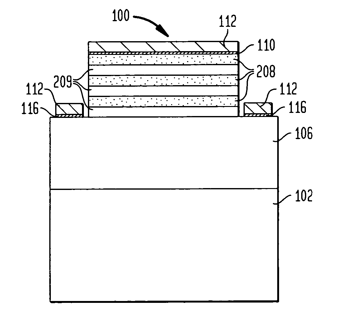
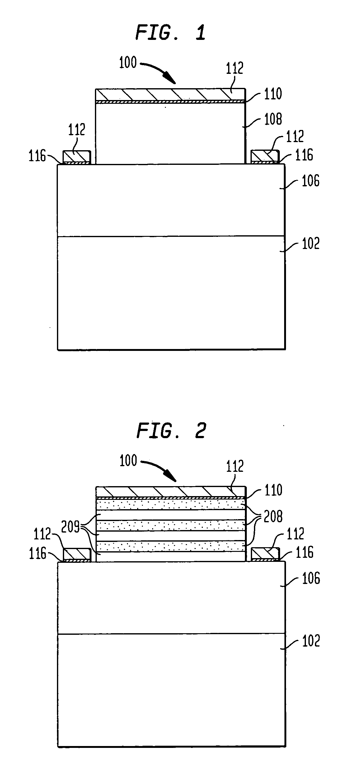
[0027] As used in the present disclosure, the term “III-V semiconductor” refers to a compound semiconductor material according to the stoichiometric formula AlaInbGacNdAsePf where (a+b+c) is about 1 and (d+e+f) is also about 1. The term “nitride semiconductor” or “nitride-based semiconductor” refers to a III-V semiconductor in which d is 0.5 or more, most typically about 0.8 or more. Preferably, the semiconductor materials are pure nitride semiconductors, i.e., nitride semiconductors in which d is about 1.0. The term “gallium nitride based semiconductor” as used herein refers to a nitride semiconductor including gallium, and most preferably including gallium as the principal metal present, i.e., having c≧0.5 and most preferably ≧0.8. The semiconductors may have p-type or n-type conductivity, which may be imparted by conventional dopants and may also result from the inherent conductivity type of the particular semiconductor material. For example, gallium nitride-based semiconductors ...


PUM


Abstract

A repeatable and uniform low doped layer is formed using modulation doping by forming alternating sub-layers of doped and undoped nitride semiconductor material atop another layer. A Schottky diode is formed of such a low doped nitride semiconductor layer disposed atop a much more highly doped nitride semiconductor layer. The resulting device has both a low on-resistance when the device is forward biased and a high breakdown voltage when the device is reverse biased.

Description

BACKGROUND OF THE INVENTION [0001] The present invention is directed to semiconductor devices and, more particularly, to nitride-based semiconductor devices, such as Schottky diodes, and to processes for making the same. [0002] Nitride-based semiconductors, such as gallium nitride and gallium nitride-based semiconductors, are widely regarded as desirable wide bandgap compound semiconductors. These materials have been adopted in optoelectronic devices, such as light-emitting diodes (LEDs), laser diodes and photodiodes, and have also been employed in non-optical electronic devices, such as field effect transistors (FETs) and field emitters. In optoelectronic devices, the wide bandgap of the material allows for emission or absorption of light in the visible-to-ultraviolet range. In electronic devices, gallium nitride and its related materials provide high electron mobility and allow for operation at very high signal frequencies. [0003] The properties of nitride-based semiconductors als...

Claims


Application Information

Patent Timeline
IPC IPC(8): H01L21/28H01L29/15H01L29/20H01L29/45H01L29/47H01L29/778H01L29/872
CPCH01L29/157H01L29/2003H01L29/872H01L29/475H01L29/7787H01L29/452
Inventor POPHRISTIC, MILANMURPHY, MICHAELSTALL, RICHARD A.SHELTON, BRYAN S.LIU, LINLINCERUZZI, ALEX D.
Owner POWER INTEGRATIONS INC
Why Eureka
Try Eureka