Memory device with different termination units for different signal frequencies
- Summary
- Abstract
- Description
- Claims
- Application Information
AI Technical Summary
Benefits of technology
Problems solved by technology
Method used
Image
Examples
Embodiment Construction
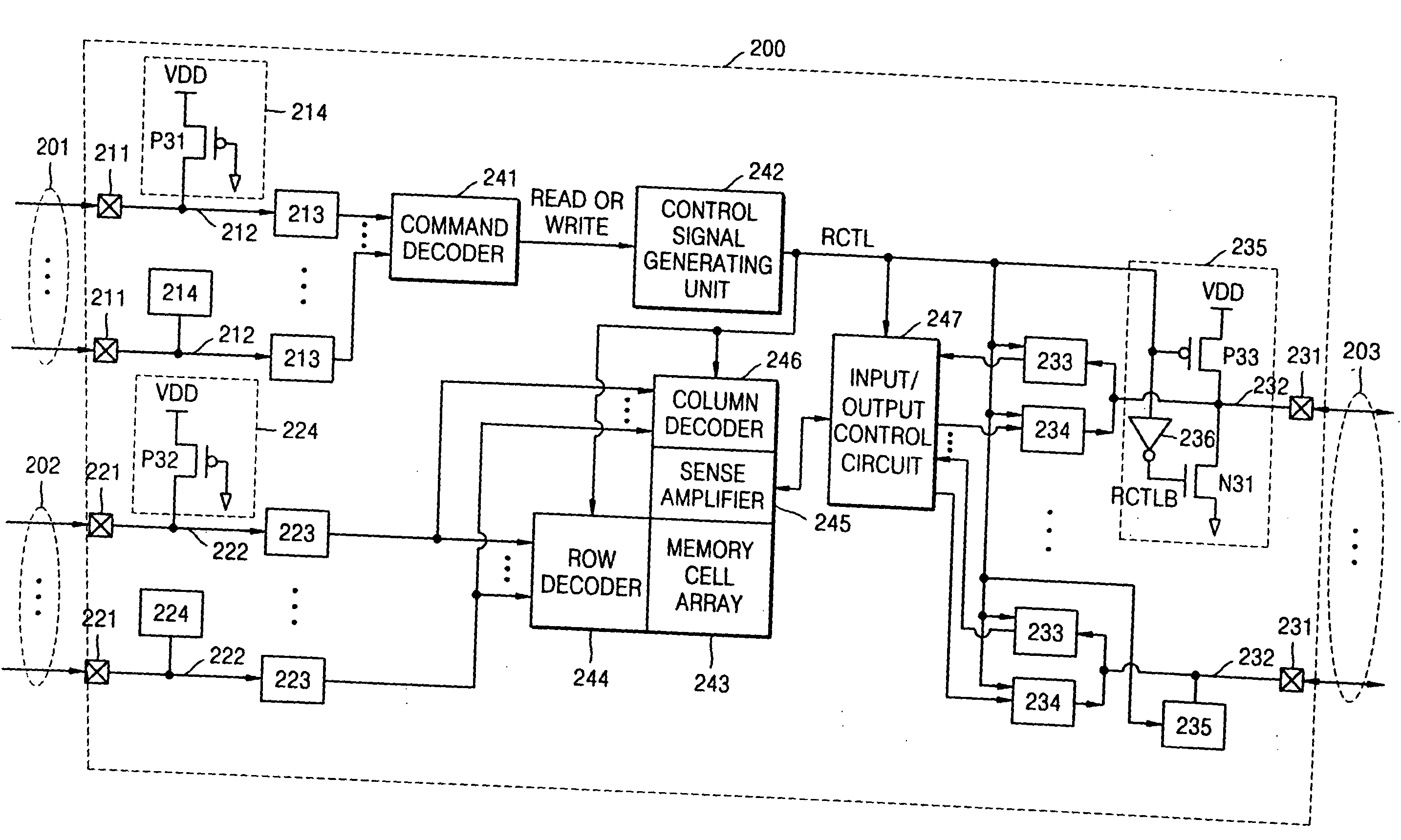
[0033]FIG. 3 is a diagram illustrating a semiconductor memory device 100 according to an embodiment of the present invention. The semiconductor memory device 100 includes components fabricated as an integrated circuit on a semiconductor substrate such as a silicon substrate in one example embodiment of the present invention. For example, the dashed lines in FIG. 3 may out-line the semiconductor substrate having the components of the memory device 100 fabricated therein.
[0034] Referring to FIG. 3, the semiconductor memory device 100 comprises control pins 101, address pins 102, and data pins 103. Each of the control pins 101 is coupled to a respective one of a first set of input / output pads 111, and each of the data pins 103 is coupled to a respective one of a second set of input / output pads 131. Each of the address pins 102 is coupled to a respective one of a third set of input / output pads 121.
[0035] The semiconductor memory device 100 further comprises external control signal inp...
PUM
 Abstract
Description
Claims
Application Information


