Micro pin grid array with wiping action

a micro pin grid array and micro pin technology, applied in the direction of coupling contact member, coupling device connection, coupling/disassembly part, etc., can solve the problems of imposing stress on solder, terminals moving relative to the contact, assembly including packages can suffer stress, etc., to facilitate the formation of conductive terminals, low cost, and large volume

Active Publication Date: 2005-08-18
TESSERA INC
View PDF76 Cites 188 Cited by
  • Summary
  • Abstract
  • Description
  • Claims
  • Application Information

AI Technical Summary

Benefits of technology

[0025] In preferred embodiments, the blank is placed atop a mold having one or more depressions formed therein and the blank is secured over the one or more depressions of the mold. Fluid pressure is desirably applied to using a pressure chamber engaged with the blank so as to force portions of the blank into the depr

Problems solved by technology

Assemblies including packages can suffer from stresses imposed by differential thermal expansion and contraction of the device and the substrate.
Where the terminals of the package are fixed relative to the chip or other device, such as by using solder, these effects tend to cause the terminals to move relative to the contact pads on the circuit board.
This can impose stresses in the solder that connects the terminals to the contact pads on the circuit board.
Testing of packaged devices poses another formidable problem.
However, it is difficult to make connections by pressing the package against a simple test fixture such as an ordinary circuit board having planar contact pads.
For example, in a BGA package, differences in the diameter of the solder balls attached to the terminals, and non-planarity of the chip carrier, may cause some of the so

Method used


Image

  • Micro pin grid array with wiping action
  • Micro pin grid array with wiping action
  • Micro pin grid array with wiping action

Examples


Embodiment Construction

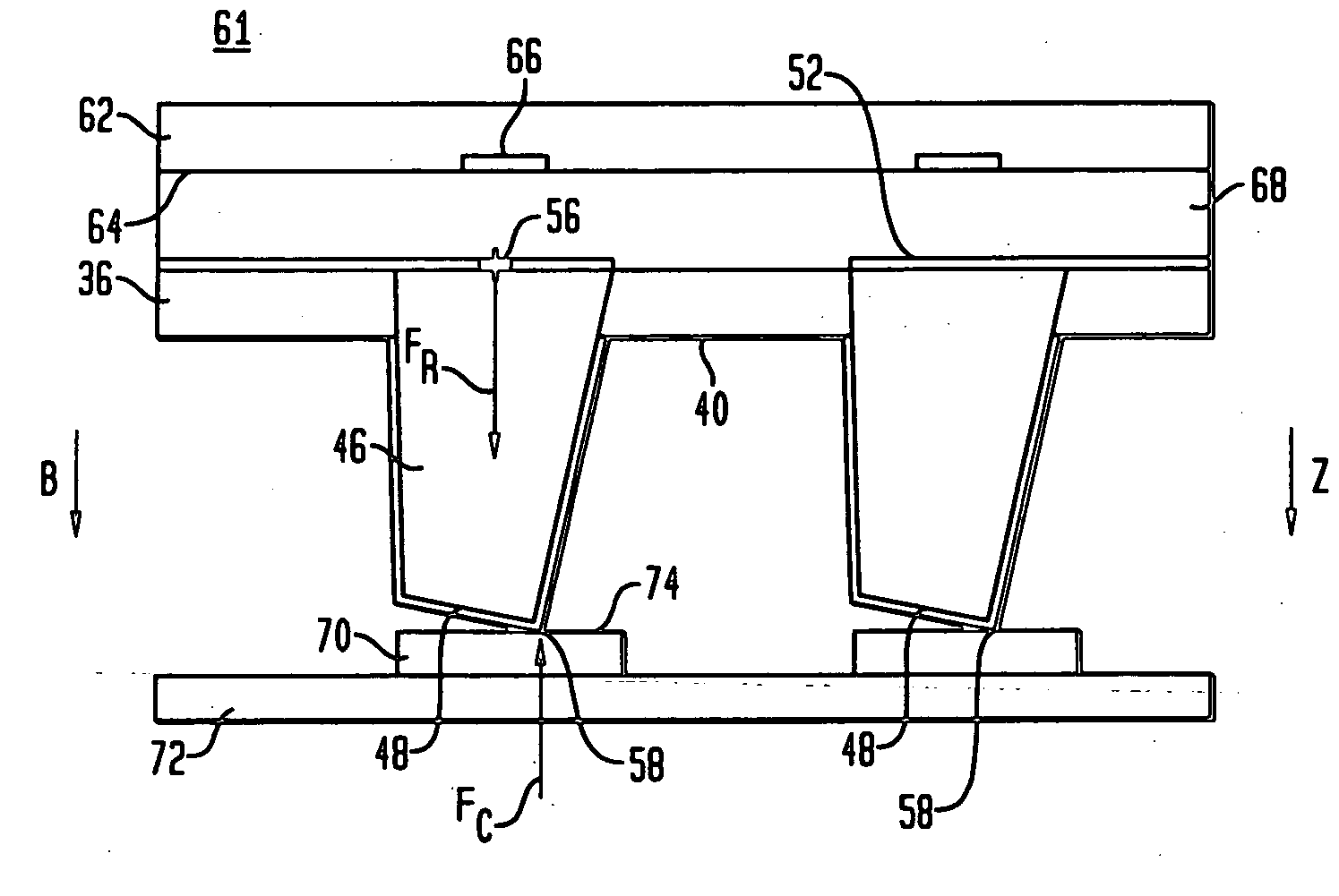
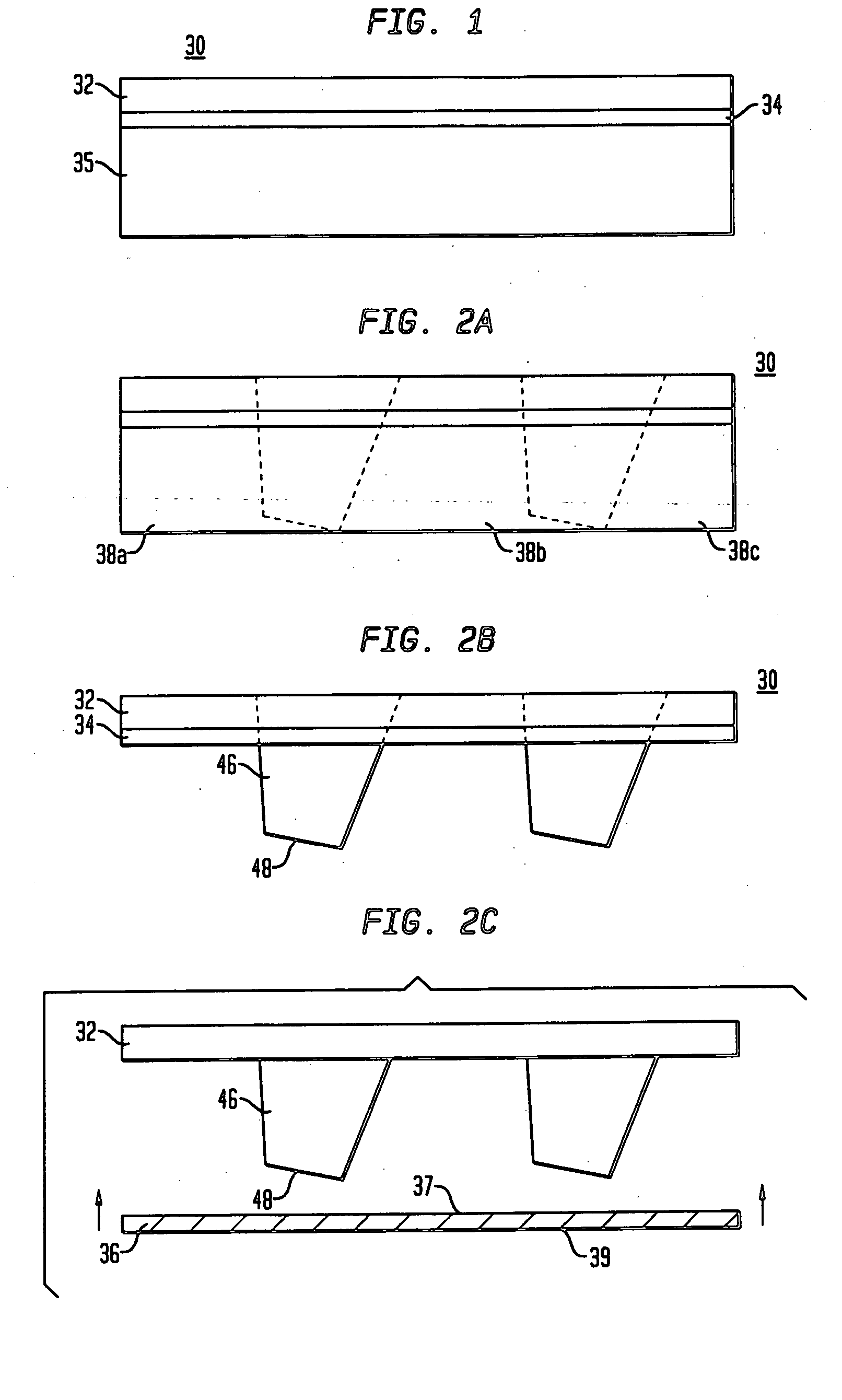
[0051] Referring to FIG. 1, in certain preferred embodiments of the present invention, a microelectronic subassembly may be fabricated by a process such as that disclosed in co-pending, commonly assigned U.S. Provisional Application No. 60 / 508,970, the disclosure of which is incorporated by reference herein. As disclosed in certain preferred embodiments of the '970 application, a metallic plate 30 includes a top layer 32 made of a conductive material, an intermediate etch stop layer 34 and a bottom layer 35 made of a conductive material. The top and bottom layers 32, 35 may include electrically conductive materials such as copper. The intermediate etch stop layer 34 may include materials such as nickel. Referring to FIGS. 2A and 2B, the bottom layer 35 of metallic plate 30 is stamped or etched to remove portions 38a, 38b and 38c of bottom layer 35 so as to form conductive terminals or posts 46. Referring to FIGS. 2B and 2C, after the posts 46 have been formed, the etch stop layer 34...


PUM


Abstract

A microelectronic package includes a mounting structure, a microelectronic element associated with the mounting structure, and a plurality of conductive posts physically connected to the mounting structure and electrically connected to the microelectronic element. The conductive posts project from the mounting structure in an upward direction, at least one of the conductive posts being an offset post. Each offset post has a base connected to the mounting structure, the base of each offset post defining a centroid. Each offset post also defines an upper extremity having a centroid, the centroid of the upper extremity being offset from the centroid of the base in a horizontal offset direction transverse to the upward direction. The mounting structure is adapted to permit tilting of each offset post about a horizontal axis so that the upper extremities may wipe across a contact pad of an opposing circuit board.

Description

CROSS REFERENCE TO RELATED APPLICATIONS [0001] The present application claims the benefit of the filing date of U.S. Provisional Application No. 60 / 533,393 filed Dec. 30, 2003, the disclosure of which is hereby incorporated herein by reference.FIELD OF THE INVENTION [0002] The present invention generally relates to microelectronic packages and more specifically to methods of making and testing microelectronic packages. BACKGROUND OF THE INVENTION [0003] Microelectronic devices such as semiconductor chips typically require many input and output connections to other electronic components. The input and output contacts of a semiconductor chip or other comparable device are generally disposed in grid-like patterns that substantially cover a surface of the device (commonly referred to as an “area array”) or in elongated rows which may extend parallel to and adjacent each edge of the device's front surface, or in the center of the front surface. Typically, devices such as chips must be ph...

Claims


Application Information

Patent Timeline
IPC IPC(8): H01L21/48H01L23/13H01R13/24H01R13/62
CPCH01L21/4846H01L23/13H01R13/2414H01R13/2464H01L2924/0002H01L2924/00
Inventor HABA, BELGACEMBEROZ, MASUDHUMPSTON, GILESPARK, JAE M.
Owner TESSERA INC
Why Eureka
Try Eureka