Wavelength converted semiconductor light emitting devices

a technology of converted semiconductors and light emitting devices, applied in the direction of discharge tubes/lamp details, discharge tubes luminescnet screens, instruments, etc., can solve the problem that white light leds based on dichromatic approaches can only be used to a limited extent for general-purpose illumination

Active Publication Date: 2005-08-25
LUMILEDS
View PDF17 Cites 183 Cited by
  • Summary
  • Abstract
  • Description
  • Claims
  • Application Information

AI Technical Summary

Benefits of technology

[0011] In accordance with embodiments of the invention, a wavelength converted semiconductor light emitting device includes a first wavelength converting material and a second wavelength converting material. The first wavelength converting material emits light having a shorter wavelength than light emitted by the second wavelength converting material. In some embodiments, the first and second wavelength convert...

Problems solved by technology

However, white light LEDs based on the dichromatic approach can only be used to a limited extent for ge...

Method used


Image

  • Wavelength converted semiconductor light emitting devices
  • Wavelength converted semiconductor light emitting devices
  • Wavelength converted semiconductor light emitting devices

Examples


Embodiment Construction

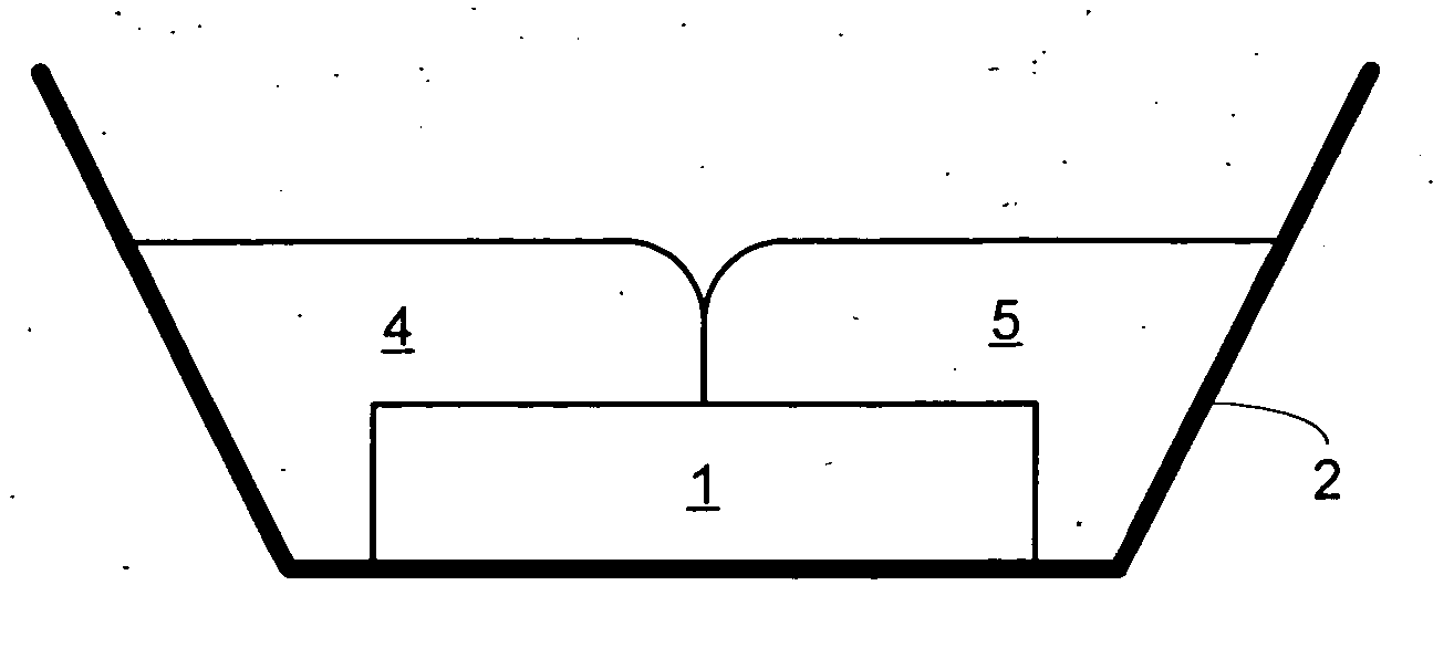
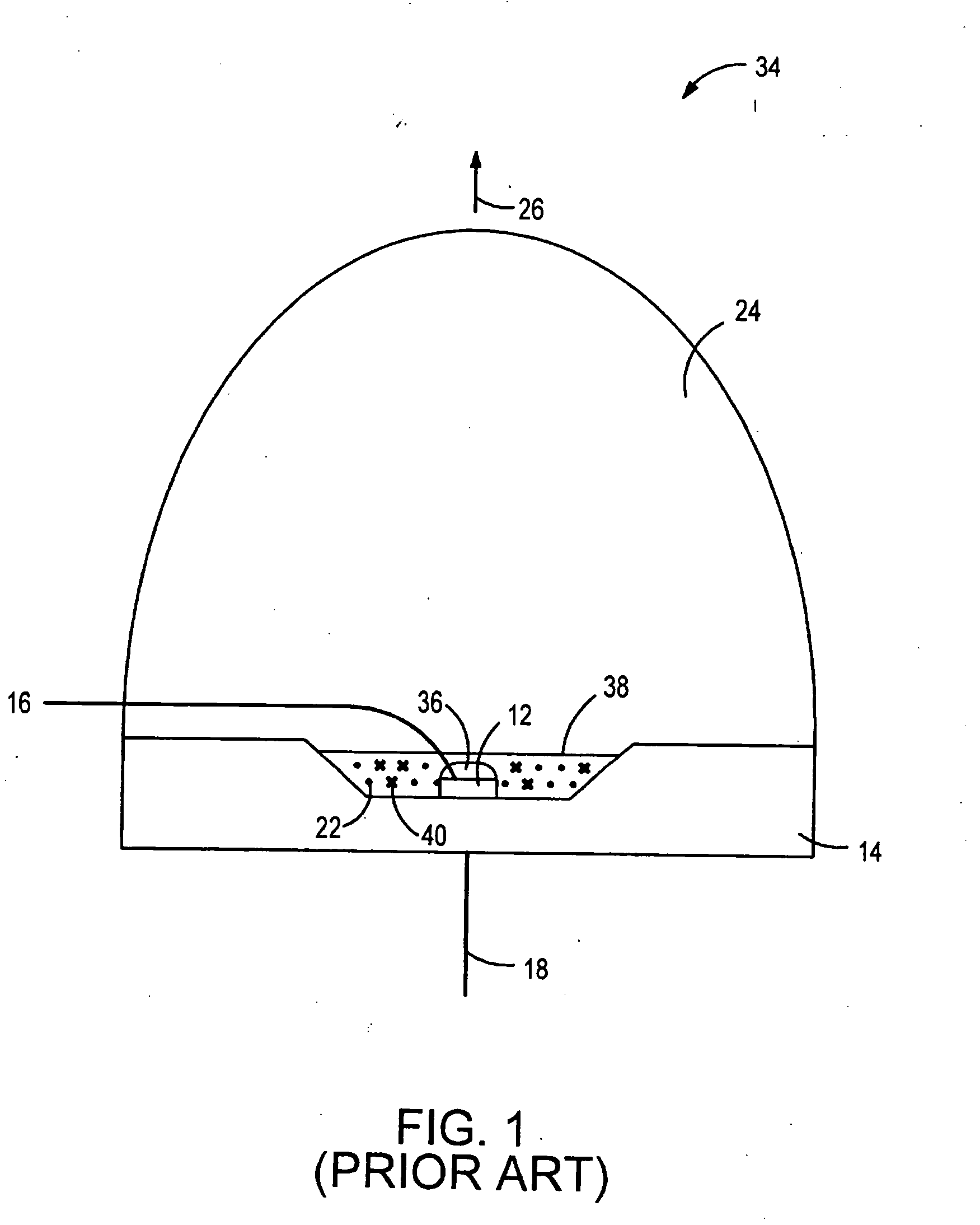
[0020] In accordance with embodiments of the invention, systems including multiple wavelength converting materials such as phosphors combined with semiconductor light emitting devices are disclosed. In the below description, “mixed” or “composite” light refers to the combination of light emitted by the semiconductor light emitting device and light emitted by all the phosphors in the system.

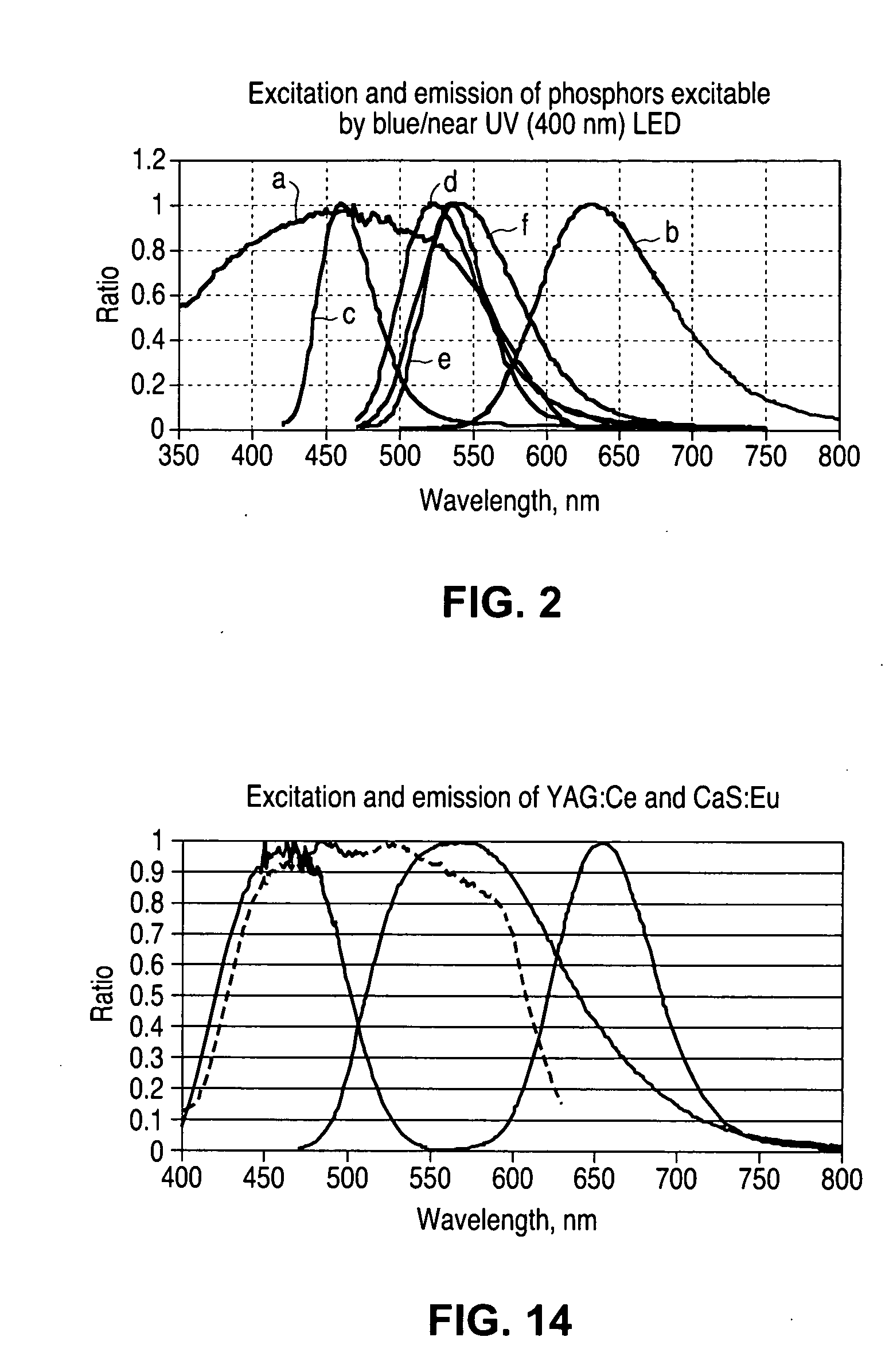
[0021] In some embodiments, a blue light emitting diode is combined with a yellow- or green-emitting phosphor and a red-emitting phosphor. Examples of suitable yellow- or green-emitting phosphors include (Lu1-x-y-a-bYxGdy)3(Al1-zGaz)5O12:Cea3+Prb3+wherein 03Al5O12:Ce3+ and Y3Al5O12:Ce3+; (Sr1-a-bCabBac)SixNyOz:Eua2+ (a=0.002-0.2, b=0.0-0.25, c=0.0-0.25, x=1.5-2.5, y=1.5-2.5, z=1.5-2.5) including, for example, SrSi2N2O2:Eu2+; (Sr1-u-v-xMguCavBax)(Ga2-y-zAlyInzS4):Eu2+ including, for example, SrGa2S4:Eu2+; and Sr1-xBaxSiO4:Eu2+. Examples of suitable red-emitting phosphors include (Ca1-xSrx)S:Eu2+ w...


PUM


Abstract

In a wavelength converted semiconductor light emitting device with at least two wavelength converting materials, the wavelength converting materials in the device are arranged relative to the light emitting device and relative to each other to tailor interaction between the different wavelength converting materials in order to maximize one or more of the luminous equivalent, color rendering index, and color gamut of the combined visible light emitted by the device.

Description

BACKGROUND [0001] 1. Field of Invention [0002] This invention relates to wavelength-converted semiconductor light-emitting devices. [0003] 2. Description of Related Art [0004] Semiconductor light-emitting devices including light emitting diodes (LEDs) are among the most efficient light sources currently available. Materials systems currently of interest in the manufacture of high-brightness light emitting devices capable of operation across the visible spectrum include Group III-V semiconductors, particularly binary, ternary, and quaternary alloys of gallium, aluminum, indium, and nitrogen, also referred to as III-nitride materials. Typically, III-nitride light emitting devices are fabricated by epitaxially growing a stack of semiconductor layers of different compositions and dopant concentrations on a sapphire, silicon carbide, III-nitride, or other suitable substrate by metal-organic chemical vapor deposition (MOCVD), molecular beam epitaxy (MBE), or other epitaxial techniques. Sa...

Claims


Application Information

Patent Timeline
IPC IPC(8): C09K11/56C09K11/59C09K11/08C09K11/62C09K11/64C09K11/80H01L33/50
CPCC09K11/0883C09K11/7731C09K11/7734C09K11/7774G02F1/133603G02F2001/133614H01L2924/0002H01L25/0753H01L33/504H01L2924/00G02F1/133614C09K11/77347C09K11/77342
Inventor MUELLER, GERD O.MUELLER-MACH, REGINA B.
Owner LUMILEDS
Why Eureka
Try Eureka