Electron emission device

a technology of electron beam and emission device, which is applied in the direction of discharge tube main electrode, discharge tube luminescnet screen, discharge tube with screen, etc., can solve the problems of reducing negatively affecting the withstand-voltage characteristic, and increasing the focusing capacity of the electron beam, so as to achieve sufficient beam focusing capacity, enhance brightness and color representation, and improve the structure of the focusing electrod

Inactive Publication Date: 2005-08-25
SAMSUNG SDI CO LTD
View PDF5 Cites 42 Cited by
  • Summary
  • Abstract
  • Description
  • Claims
  • Application Information

AI Technical Summary

Benefits of technology

[0012] In accordance with the present invention, an electron emission device is provided which improves the structure

Problems solved by technology

Whether a grid electrode or focusing electrode is used, increases in the focusing capacity of the electron beam negatively affect the withstand-voltage characteristic, i.e. the capacity to intercept electric fields emanating from the anode electrode.
Similarly, improvements in the withstand-voltage characteristic negatively affect the focusing capacity of the electron beam.
However, when this is done, the focusing capacity is reduced and the electric field of the anode e

Method used


Image

  • Electron emission device
  • Electron emission device
  • Electron emission device

Examples


Embodiment Construction

[0028] The present invention will be described more fully hereinafter with reference to the accompanying drawings, in which preferred embodiments of the invention are shown.

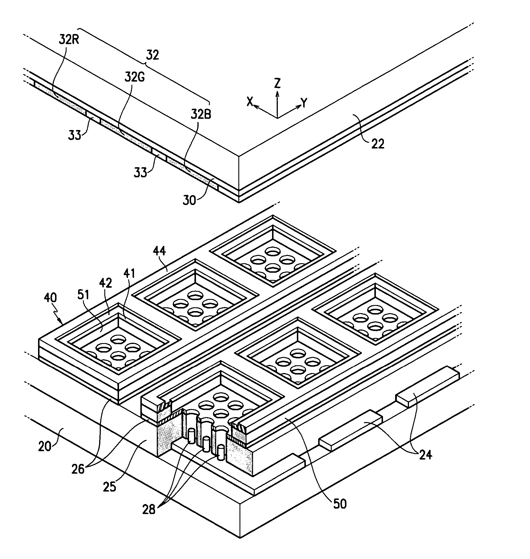
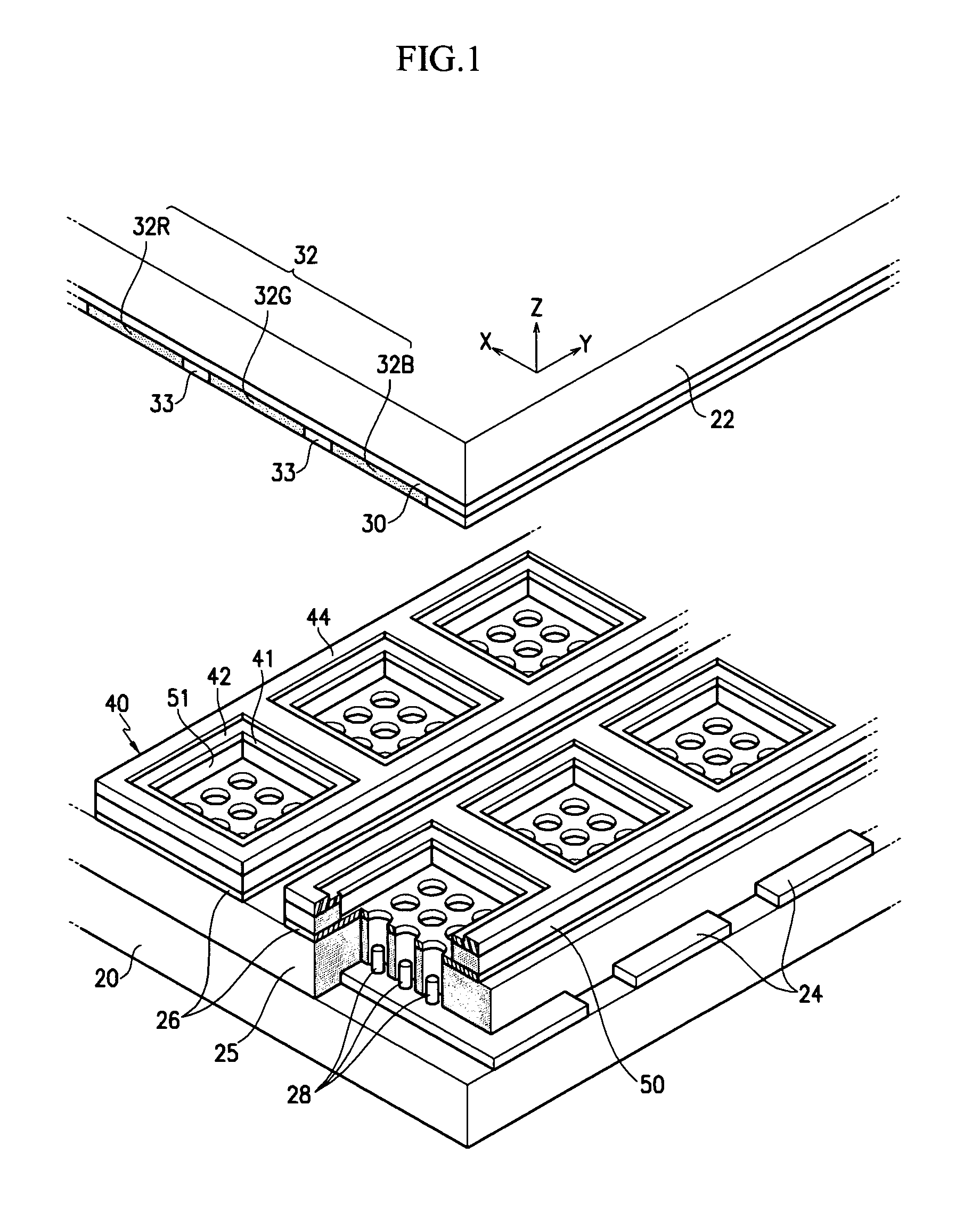
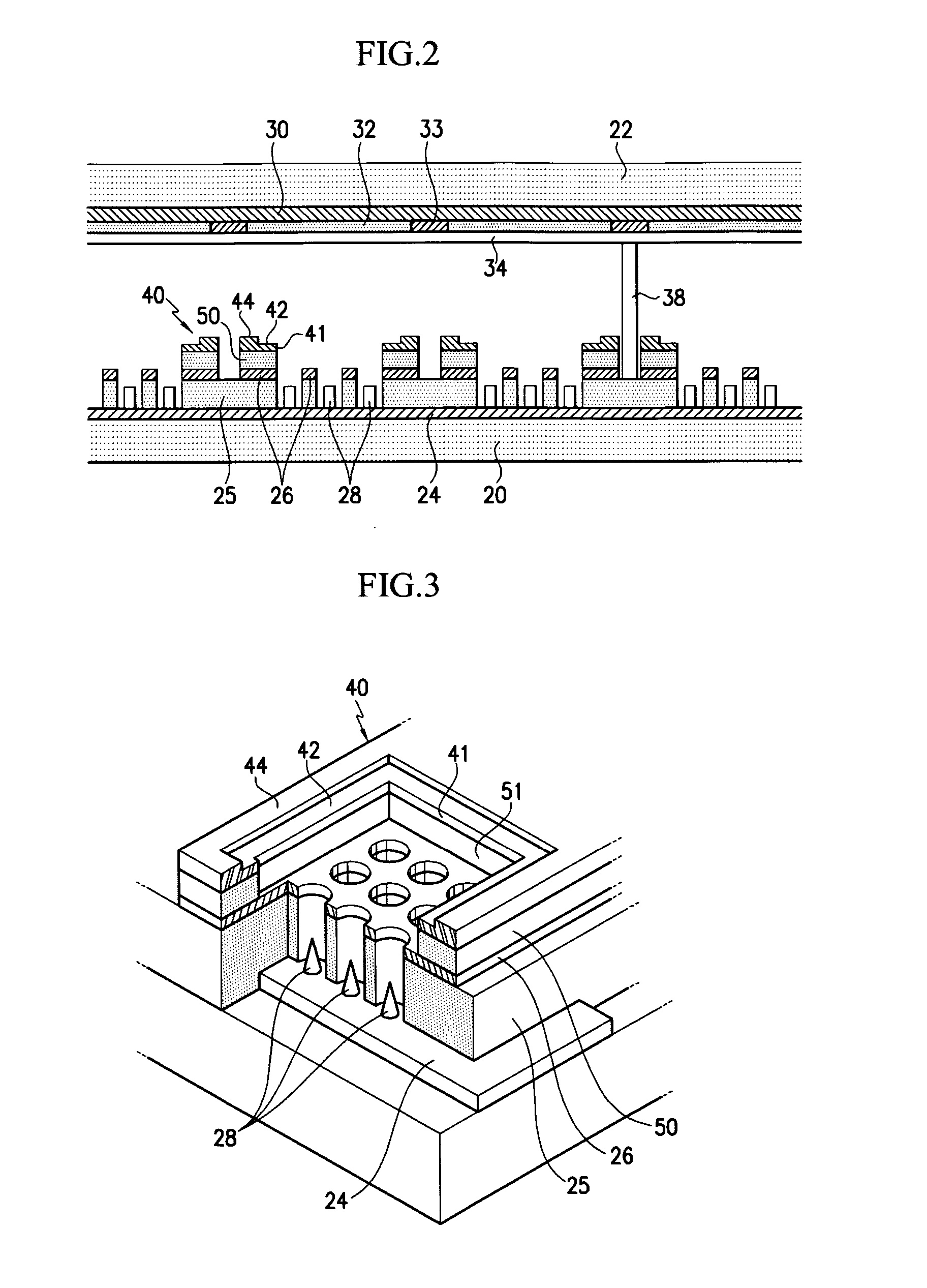
[0029] As shown in FIGS. 1 and 2, an electron emission device according to a first embodiment of the present invention includes first and second substrates 20 and 22, respectively, positioned facing each other and separated from each other by a predetermined distance, thereby forming a vacuum vessel.

[0030] An electron emission unit is provided on the first substrate 20, and an image display unit is provided on the second substrate 22. The electron emission unit emits electrons to the image display unit, which thereby emits light, displaying the desired images.

[0031] The electron emission unit on the first substrate 20 comprises a plurality of cathode electrodes 24 arranged on the first substrate 20 and spaced apart by a predetermined distance. Electron emission regions 28 are positioned on the cathode electrod...


PUM


Abstract

An electron emission device is provided comprising first and second substrates facing each other and separated from each other by a predetermined distance. An electron emission unit is disposed on the first substrate, and an image display unit is disposed on the second substrate. A focusing electrode comprising a plurality of beam-guide holes is disposed between the first and second substrates. The portion of the focusing electrode located near a beam-guide hole comprises a thin layer. The remainder of the focusing electrode comprises a thick layer having a thickness larger than the thickness of the thin layer.

Description

CROSS-REFERENCE TO RELATED APPLICATION [0001] This application claims the benefit of and priority to Korean Patent Application No. 10-2004-0012636 filed on Feb. 25, 2004 in the Korean Intellectual Property Office, the entire disclosure of which is incorporated herein by reference. FIELD OF THE INVENTION [0002] The present invention relates to an electron emission device, and in particular, to a focusing electrode for an electron emission device. BACKGROUND OF THE INVENTION [0003] Generally, electron emission devices are classified into two types. In the first type, a hot cathode is used as an electron emission source. In the second type, a cold cathode is used as the electron emission source. [0004] Known electron emission devices of the second type include a field emitter array (FEA) type, a surface conduction emitter (SCE) type, a metal-insulator-metal (MIM) type, a metal-insulator-semiconductor (MIS) type, and a ballistic electron surface emitting (BSE) type. [0005] Electron emis...

Claims


Application Information

Patent Timeline
IPC IPC(8): H01J1/30H01J29/04H01J1/304H01J1/62H01J3/02H01J29/46H01J29/48H01J31/12
CPCH01J3/021H01J31/127H01J29/481H01J29/467B60M1/20B60L2200/26B60Y2200/30
Inventor CHANG, CHEOL-HYEON
Owner SAMSUNG SDI CO LTD
Why Eureka
Try Eureka