
Display device and display panel device

a technology of display panel and display device, which is applied in the field of display devices, can solve the problems of limited power consumption in the light emission region of the screen unit area, and achieve the effects of reducing the weight of the device, reducing the risk of overheating of the filter and the display panel, and prolonging the optical function

Inactive Publication Date: 2005-08-25
MAXELL HLDG LTD
View PDF3 Cites 12 Cited by
  • Summary
  • Abstract
  • Description
  • Claims
  • Application Information

AI Technical Summary

Benefits of technology

[0010] An object of the present invention is to reduce a weight of the device while suppressing excessive temperature rise of the filter and the plasma display panel so that a long life of the filter and stability of a display can be realized. Another object is to prevent overheating of an outer surface of the device so that safety about outer surface temperature during operation can be ensured.
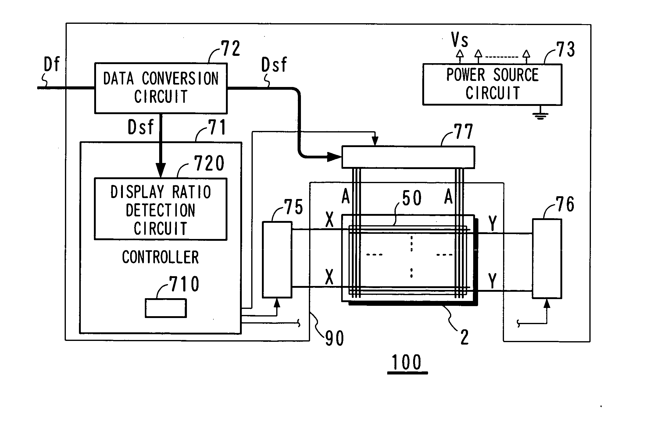
[0011] According to an aspect of the present invention, a display device includes a plasma display panel having a screen including a plurality of cells, a functional sheet having at least an optical filter function to light emitted from the screen and being brought into intimate contact with a front surface of the plasma display panel, and a drive voltage output circuit for giving the screen a drive voltage pulse train that generates display discharge plural times corresponding to a gradation. The functional sheet has a structure in which heat diffusion is superior to heat insulation between the plasma display panel and outside air. In addition, the display device includes a controller for controlling the drive voltage pulse train so that power consumption in a unit area in a light emission region within the screen is limited under a set value when one image is displayed.
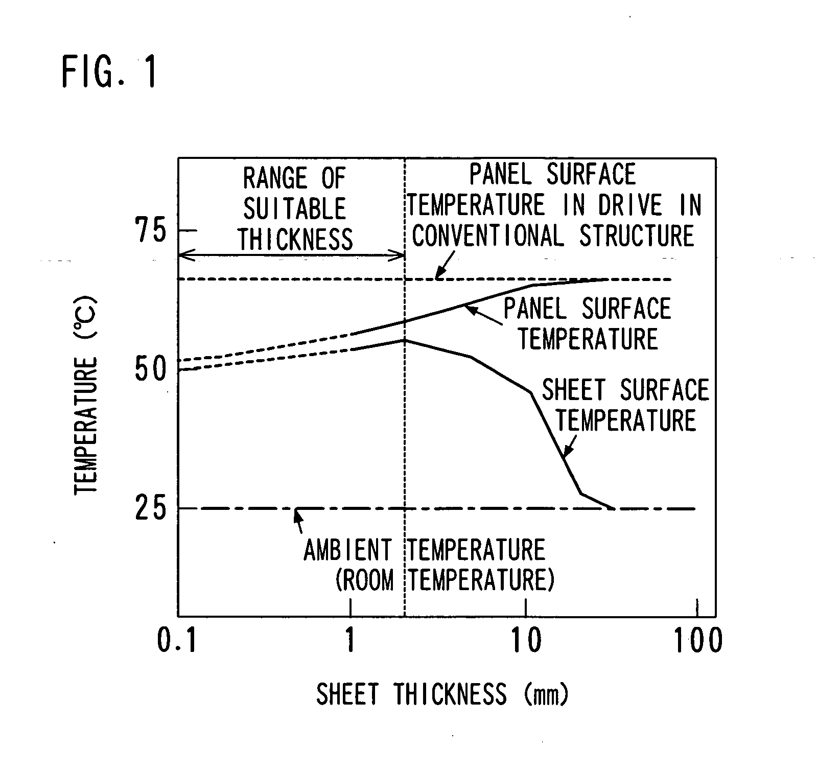
[0013] In addition, the inventor found a temperature on the surface of the panel and a temperature on the surface of the sheet are determined substantially not by total power supplied to the plasma display panel but by power consumption per a unit area in a light emission region within the screen (this is called a local power density). Namely, when the local power density is controlled to an appropriate upper limit value, excessive heat can be prevented both on the plasma display panel and on the functional sheet.
[0015] Adding to the above-mentioned selection of a thickness of the functional sheet and limitation of the local power density, a layer structure of the functional sheet is devised so that a long life of the optical function can be achieved. A layer containing a material that is apt to occur thermal deterioration (for example, a coloring matter for selecting a wavelength) is arranged as close as possible to the front surface so that it is away from the plasma display panel that is a heat source. Furthermore, the layer that is arranged on the rear side of the layer that is apt to occur thermal deterioration is made thick, so that temperature rise of the material that is apt to occur thermal deterioration can be reduced.
[0016] According to the present invention, a weight of the device is reduced while excessive temperature rise of the filter and the plasma display panel can be suppressed so that a long life of the filter and stability of a display can be realized.
[0017] In addition, overheating of an outer surface of the device is prevented so that safety about outer surface temperature during operation can be ensured.

Problems solved by technology

In addition, the display device includes a controller for controlling the drive voltage pulse train so that power consumption in a unit area in a light emission region within the screen is limited under a set value when one image is displayed.

Method used


Image

  • Display device and display panel device
  • Display device and display panel device
  • Display device and display panel device

Examples


example 1

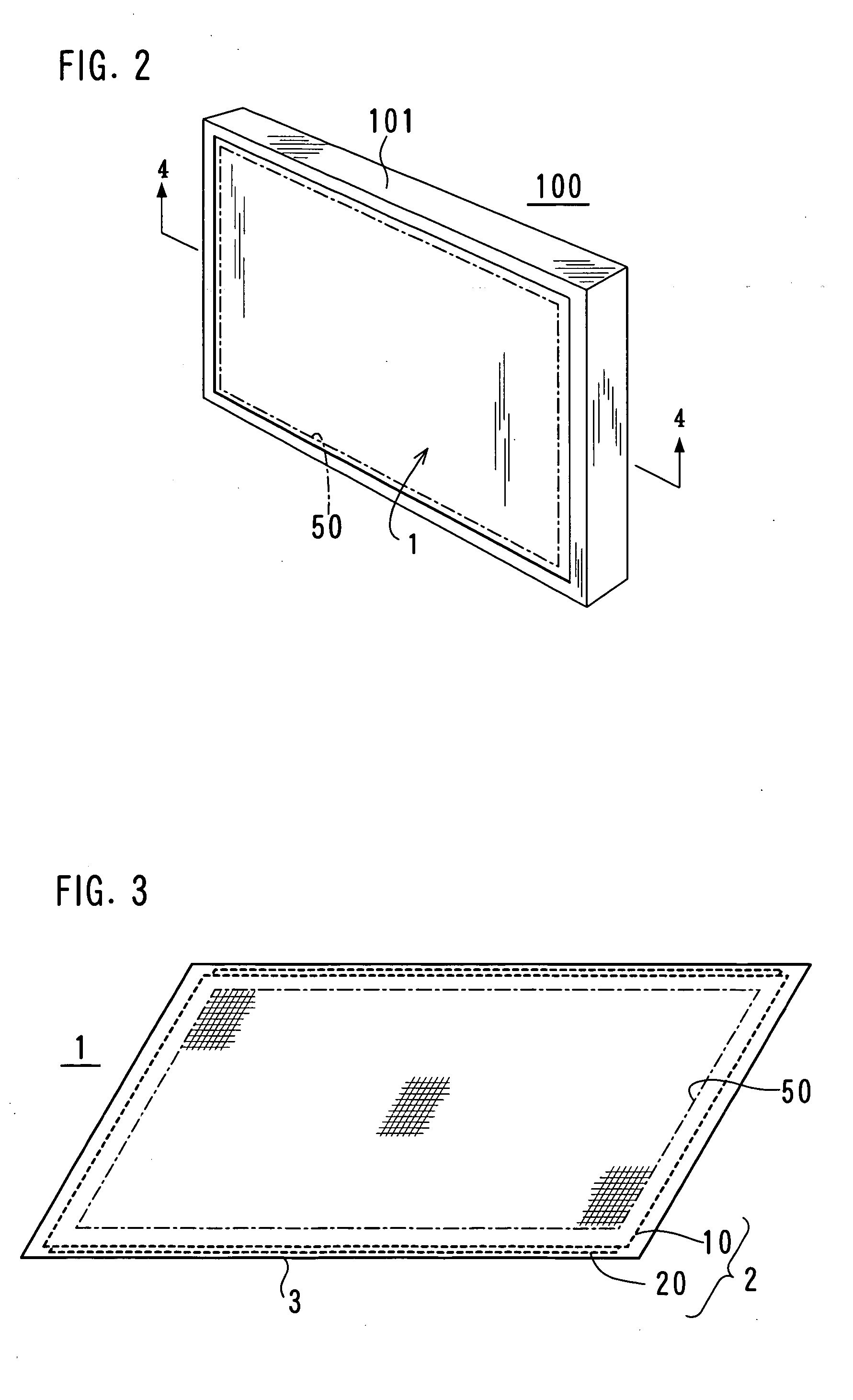
[0042]FIG. 2 shows an appearance of a display device according to the present invention. A display device 100 is a flat type display having a 32-inch diagonal screen 50. A dimension of the screen 50 is 0.72 meters in the horizontal direction and 0.40 meters in the vertical direction. A facing cover 101 that defines a plane size of the display device 100 has an opening that is larger than the screen 50, so that a front face of a display panel device 1 is exposed in part.

[0043]FIG. 3 shows a structure of the display panel device. The display panel device 1 includes a plasma display panel 2 that is a device that constitutes a screen and a front sheet 3 that is glued directly on the front face of the plasma display panel 2 to be a display face. The front sheet 3 is a sheet-like structure corresponding to a functional sheet according to the present invention. The plasma display panel 2 is a self-luminous type device that emits light by gas discharge, which includes a front face plate 10...

example 2

[0086]FIG. 18 shows a second example of a structure of the display device. A basic structure of the display device 200 is the same as the above-mentioned display device 100 except for a screen size. In FIG. 18 and the following diagrams, structural elements denoted by the same reference numerals as in FIG. 4 are the same structural elements as of the display device 100.

[0087] The display device 200 has a 42-inch diagonal screen. A dimension of the screen is 0.92 meters in the horizontal direction and 0.52 meters in the vertical direction. The display panel device 5 that is a screen module of the display device 200 includes a plasma display panel 4 and a front sheet 6. The plasma display panel 4 includes a front face plate 11 and a rear face plate 21, and the front sheet 6 includes a front portion 6A and a rear portion 6B.

[0088] In the display device 200, a plane size of the front portion 6A is larger than the above-mentioned example, four sides of the front portion 6A are bent to ...

example 3

[0097]FIG. 21 shows a third example of a structure of the display device. A structure of a display device 300 is substantially the same as the above-mentioned display device 200.

[0098] The display device 300 is characterized in that the inner rim of the front face of the facing cover 301 is close to a screen area, and sound absorbing members 351 and 352 are arranged between the facing cover 301 and the front sheet 6. The sound absorbing members 351 and 352 are glued on the facing cover 301 in advance, and the display panel device 5 is covered with the facing cover 301 so that the sound absorbing members 351 and 352 are pressed onto the front sheet 6. As the sound absorbing members 351 and 352 are flexible sponge, no excessive force is applied to the plasma display panel 4. As audible sound noises due to vibration of the plasma display panel 4 (called an abnormal sound) increases at a peripheral portion of the plasma display panel 4, the noises can be reduced substantially by arrang...


PUM


Abstract

A functional sheet is brought into intimate contact with a front surface of a plasma display panel, and the functional sheet has a structure in which heat diffusion is superior to heat insulation between the plasma display panel and outside air. In addition, a display device includes a controller for controlling a drive voltage pulse train so that power consumption in a unit area in a light emission region within the screen is limited under a set value when one image is displayed.

Description

BACKGROUND OF THE INVENTION [0001] 1. Field of the Invention [0002] The present invention relates to a display device having a display panel device including a plasma display panel and a functional sheet that is brought into intimate contact with a front surface of the plasma display panel. [0003] 2. Description of the Prior Art [0004] Technology development of a plasma display panel (PDP) that is a self-luminous device is directed to a large screen for providing more powerful display. One of the important tasks for a large screen is weight reduction of the panel. [0005] In general, a display device including a plasma display panel has a rigid filter plate having a base of a tempered glass. This filter plate is arranged in front of the plasma display panel with air gap. The filter plate has various functions of adjusting a display color optically, preventing reflection of external light, shielding electromagnetic waves, and shielding near infrared rays concerning displaying operatio...

Claims


Application Information

Patent Timeline
Patent Type & Authority Applications(United States)
IPC IPC(8): G09F9/00H04N5/66G09F9/313G09G3/10G09G3/20G09G3/288G09G3/291G09G3/294G09G3/298H04N5/72
CPCG09G3/2944G09G2330/021H05K7/20972G09G2360/16G09G2330/045A63F7/02G07F17/32A63F2250/142
Inventor HORI, NOBUYUKIKAWANAMI, YOSHIMIOHSAWA, ATSUONAMIKI, FUMIHIRO
Owner MAXELL HLDG LTD
Learn More