Magnetoresistive element and magnetic memory device

Inactive Publication Date: 2005-08-25
TOSHIBA MEMORY CORP
View PDF30 Cites 28 Cited by
  • Summary
  • Abstract
  • Description
  • Claims
  • Application Information

AI Technical Summary

Benefits of technology

[0010] An object of the present invention is to provide a magnetoresistive element of a tunnel junction type and a magnetic memory device in that reduction in the MR change can be made low even when an applied voltage is increased to obtain required output voltage, that have

Problems solved by technology

However, there is a problem that the magnetoresistance (MR) change is considerably decreased in the ferromagnetic single tunnel junction element, when a voltage to be applied is increased to obtain required output voltage (Phys. Rev. Lett. 74, 3273 (1995)).
However, such an element also has a similar problem that the MR change is considerably decreased when an applied voltage is increased to obtain required output voltage.
Moreover, as the ferromagnetic double tunnel junction element of the above structure has no ferromagnetic layer pinned with an antiferromagnetic layer, there is a problem that the output is gradually decreased owing to rotation of a part of magnetic moments in a magnetization pinned layer by performing writing several times when it is used for MRAM and the like.
However, as the element has no ferromagnetic layer pinned with an antiferromagnetic layer, there is a problem that the output is gradually decreased owing to rotation of a part of magnetic moments in a magnetization pinned layer by performing writing several times when it is used

Method used


Image

  • Magnetoresistive element and magnetic memory device
  • Magnetoresistive element and magnetic memory device
  • Magnetoresistive element and magnetic memory device

Examples


embodiment 1

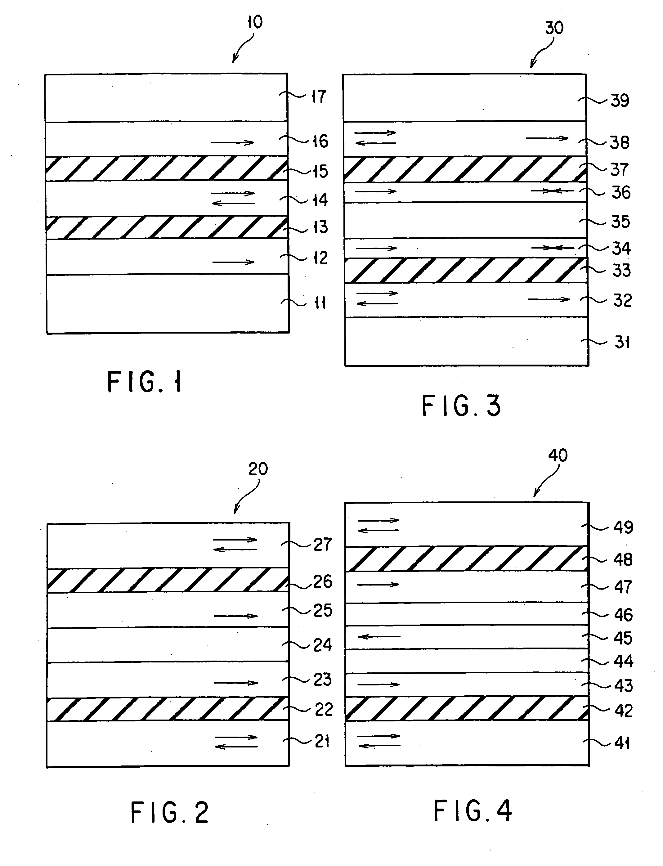
[0132] An embodiment, where two kinds of ferromagnetic double tunnel junction elements (sample A, and B) with the structure shown in FIG. 1 were formed on a Si / SiO2 substrate or SiO2 substrate, will be described below.

[0133] The sample A has a structure sequentially stacked with a TaN underlayer, a first antiferromagnetic layer of a two-layered film of Fe—Mn / Ni—Mn, a first ferromagnetic layer of CoFe, a first dielectric layer of Al2O3, a second ferromagnetic layer of Co9Fe, a second dielectric layer of Al2O3, a third ferromagnetic layer of CoFe, a second antiferromagnetic layer of a two-layered film of Ni—Fe / Fe—Mn, and a protective layer of Ta.

[0134] The sample B has a structure sequentially stacked with a TaN underlayer, a first antiferromagnetic layer of Ir—Mn, a first ferromagnetic layer of Co—Fe, a first dielectric layer of Al2O3, a second ferromagnetic layer of a three-layered film of CoFe / Ni—Fe / CoFe, a second dielectric layer of Al2O3, a third ferromagnetic layer of CoFe, a ...

embodiment 2

[0149] An embodiment, where two kinds of ferromagnetic double tunnel junction elements (sample A2, and B2) with the structure shown in FIG. 2 were formed on a Si / SiO2 substrate or SiO2 substrate, will be described below.

[0150] The sample A2 has a structure sequentially stacked with a TaN underlayer, a first ferromagnetic layer of a two-layered film of Ni—Fe / CoFe, a first dielectric layer of Al2O3, a second ferromagnetic layer of CoFe, an antiferromagnetic layer of Ir—Mn, a third ferromagnetic layer of CoFe, a second dielectric layer of Al2O3, a fourth ferromagnetic layer of a two-layered film of CoFe / Ni—Fe, and a protective layer of Ta.

[0151] The sample B2 has a structure sequentially stacked with a TaN underlayer, a first ferromagnetic layer of a three-layered film of Ni—Fe / Ru / CoFe, a first dielectric layer of Al2O3, a second ferromagnetic layer of a two-layered film of CoFe / Ni—Fe, a first antiferromagnetic layer of Fe—Mn, a third ferromagnetic layer of a two-stacked film of Ni—F...

embodiment 3

[0166] An embodiment, where two kinds of ferromagnetic double tunnel junction elements (sample A3, and B3) with the structure shown in FIG. 3 were formed on a Si / SiO2 substrate or SiO2 substrate, will be described below.

[0167] The sample A3 has a structure sequentially stacked with a TaN underlayer, a first antiferromagnetic layer of Ir—Mn, a first ferromagnetic layer of Co—Fe, a first dielectric layer of Al2O3, a second ferromagnetic layer of Co—Fe—Ni, a second antiferromagnetic layer of Fe—Mn, a third ferromagnetic layer of Co—Fe—Ni, a second dielectric layer of Al2O3, a fourth ferromagnetic layer of Co—Fe, an third antiferromagnetic layer of Ir—Mn, and a protective layer of Ta.

[0168] The sample B3 has a structure sequentially stacked with a TaN underlayer, a first antiferromagnetic layer of Ir—Mn, a first ferromagnetic layer of a three-layered film of Co—Fe / Ru / Co—Fe, a first dielectric layer of Al2O3, a second ferromagnetic layer of a two-layered film of CoFe / Ni—Fe, a second an...


PUM


Abstract

A magnetoresistive element has a ferromagnetic double tunnel junction having a stacked structure of a first antiferromagnetic layer/a first ferromagnetic layer/a first dielectric layer/a second ferromagnetic layer/a second dielectric layer/a third ferromagnetic layer/a second antiferromagnetic layer. The second ferromagnetic layer that is a free layer consists of a Co-based alloy or a three-layered film of a Co-based alloy/a Ni—Fe alloy/a Co-based alloy. A tunnel current is flowed between the first ferromagnetic layer and the third ferromagnetic layer.

Description

CROSS-REFERENCE TO RELATED APPLICATIONS [0001] This application is based upon and claims the benefit of priority from the prior Japanese Patent Applications No. 11-262327, filed Sep. 16, 1999; No. 11-263741, filed Sep. 17, 1999; No. 2000-265663, filed Sep. 1, 2000; and No. 2000-265664, filed Sep. 1, 2000, the entire contents of which are incorporated herein by reference. BACKGROUND OF THE INVENTION [0002] The present invention relates to a magnetoresistive element having ferromagnetic double tunnel junction, and, a magnetic memory device using the same. [0003] The magnetoresistance effect is a phenomenon that electrical resistance changes when a magnetic field is applied to a ferromagnetic material. As the magnetoresistive element (MR element) using the above effect has superior temperature stability within a wide temperature range, it has been used for a magnetic head and a magnetic sensor, and the like. Recently, a magnetic memory device (a magnetoresistive memory or a magnetic ra...

Claims


Application Information

Patent Timeline
IPC IPC(8): G01R33/09G11B5/39G11C11/15G11C11/16H01F10/32H01L21/8246H01L27/22H01L43/08
CPCB82Y10/00Y10T428/1121G01R33/093G11B5/3903G11B5/3909G11C11/15G11C11/16H01F10/3254H01F10/3263H01F10/3272H01F10/3281H01L27/224H01L27/228H01L43/08Y10T428/115B82Y25/00H10B61/10H10B61/22H10N50/10
Inventor INOMATA, KOICHIRONAKAJIMA, KENTAROSAITO, YOSHIAKISAGOI, MASAYUKIKISHI, TATSUYA
Owner TOSHIBA MEMORY CORP
Why Eureka
Try Eureka