Semiconductor device and method of fabricating the same

a technology of semiconductor devices and semiconductors, applied in semiconductor devices, semiconductor/solid-state device details, electrical apparatus, etc., can solve problems such as tddb failure and tddb failur

Inactive Publication Date: 2005-09-01
RENESAS ELECTRONICS CORP
View PDF12 Cites 12 Cited by
  • Summary
  • Abstract
  • Description
  • Claims
  • Application Information

AI Technical Summary

Problems solved by technology

Under accelerating trends in micronization of the semiconductor devices and concomitant narrowing of the distance between interconnects being expected for the future, even the above-described conventional configuration of the semiconductor device may result in TDDB (time-dependent dielectric breakdown) failure, due to leakage current between the interconnects applied with an electric field.
In this sort of configuration having the distance between the interconnects shorter than the previous, the electric field will be more likely to concentrate to the upper portion of the interconnects when applied with voltage, and will cause the TDDB failure.

Method used


Image

  • Semiconductor device and method of fabricating the same
  • Semiconductor device and method of fabricating the same
  • Semiconductor device and method of fabricating the same

Examples


first embodiment

[0050] The following paragraphs will explain a semiconductor device of the first embodiment.

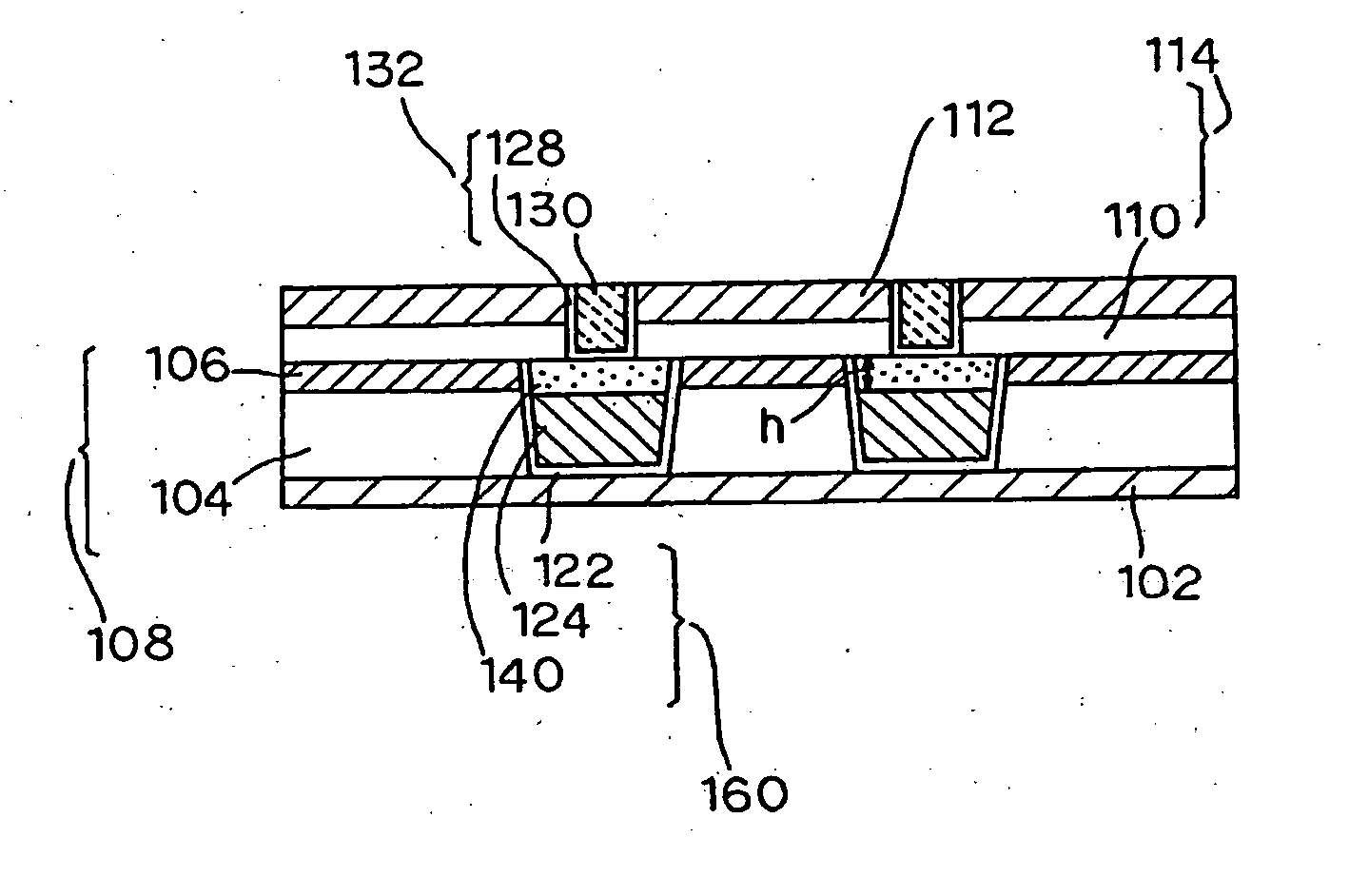
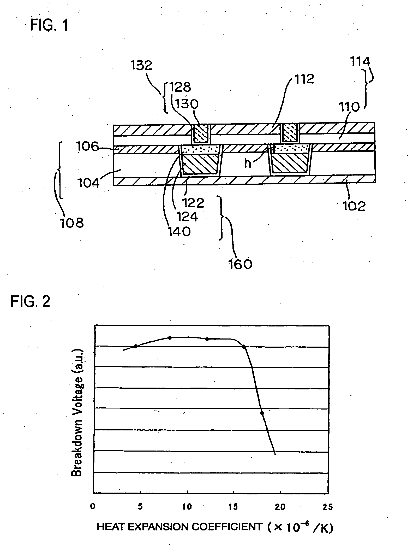
[0051]FIG. 1 is a sectional structural view showing an exemplary configuration of the semiconductor device of this embodiment. It is to be noted that the structure covering the semiconductor substrate up to the layer just below a stopper insulating layer 102 is the same as the conventional structure, and has been omitted from the illustration.

[0052] Similarly to as shown in the conventional structure, the semiconductor device has, on the stopper insulating layer 102, an insulating interlayer 108 composed of a low-k layer 104 and a hard mask layer 106. In this embodiment, a barrier metal layer 122 is formed on the bottom and side wall of the interconnect-forming grooves formed in the insulating interlayer 108, and a Cu layer 124 and a low-expansion metal layer 140 (as a metal layer), which is a metal layer having a heat expansion coefficient smaller than that of Cu, are layered in this order...

second embodiment

[0081] The present embodiment relates to a case in which the low-expansion metal layer is formed to a level of height above the upper surface of the hard mask layer.

[0082] A semiconductor device of the present embodiment will be explained.

[0083]FIG. 6 is a sectional structural view showing an exemplary configuration of the semiconductor device of the present embodiment. It is to be noted that any configurations similar to those in the first embodiment will be given with the same reference numerals, omitting the explanations therefor.

[0084] An interconnects 162 in the semiconductor device of the present embodiment are configured so that a low-expansion metal layer 142 (as a metal layer) on the Cu layer 124 is formed up to a level of height higher than the upper surface of the hard mask layer 106. The low-expansion metal layer 142 partially blocks the boundary between the insulating interlayer 108 and an insulating interlayer 114. In view of preventing the resistance of the interco...

third embodiment

[0091] The present embodiment relates to a case where the hard mask layer, formed on the insulating interlayer shown in the second embodiment, is omitted.

[0092] Next paragraphs will explain the semiconductor device of the present embodiment.

[0093]FIG. 8 is a sectional structural view showing an exemplary configuration of the semiconductor device of the present embodiment. It is to be noted that any configurations similar to those in the second embodiment will be given with the same reference numerals, omitting the detailed explanations therefor.

[0094] An insulating interlayer 109 of the present embodiment is configured by a low-k layer. On the low-k layer, the insulating interlayer 114 is formed without being underlain by the hard mask layer. Similarly to as described in the second embodiment, the barrier metal layer 122, Cu layer 124, and low-expansion metal layer 142 are formed in the interconnect-forming grooves, to thereby form the interconnects 162. The low-expansion metal l...


PUM

PropertyMeasurementUnit
dielectric constantaaaaaaaaaa
distanceaaaaaaaaaa
thickaaaaaaaaaa

Abstract

A semiconductor device having interconnects is reduced in leakage current between the interconnects and improved in the TDDB characteristic. It includes an insulating interlayer 108, and interconnects 160 filled in grooves formed in the insulating interlayer, including a copper layer 124 mainly composed of copper, having the thickness smaller than the depth of the grooves, and a low-expansion metal layer 140, which is a metal layer having a heat expansion coefficient smaller than that of the copper layer, formed on the copper layer.

Description

[0001] This application is based on Japanese patent application No. 2004-053620 the content of which is incorporated hereinto by reference. DISCLOSURE OF THE INVENTION [0002] 1. Field of the Invention [0003] The present invention relates to a semiconductor device having interconnects, and a method of fabricating the same. [0004] 2. Related Art [0005] Conventional semiconductor device uses interconnects configured by forming interconnect-forming grooves in an insulating interlayer, and by filling the interconnect-forming grooves with a metal layer such as a copper (Cu) layer (see Japanese Laid-Open Patent Publication No. 2001-176965, for exapmle). [0006]FIG. 11 is a sectional structural view of an exemplary configuration of a conventional semiconductor device. [0007] As shown in FIG. 11, the semiconductor device has semiconductor elements such as transistors, resistors, capacitors and so forth, all of which not shown, formed on a semiconductor substrate 100, and thereon a stopper ins...

Claims


Application Information

Patent Timeline
Patent Type & Authority Applications(United States)
IPC IPC(8): H01L23/52H01L21/288H01L21/3205H01L21/44H01L21/4763H01L21/768H01L23/48H01L23/532H01L29/40
CPCH01L21/288H01L21/76849H01L23/53295H01L21/76879H01L23/53238H01L21/76877H01L2924/0002H01L2924/00
Inventor KUROKAWA, TETSUYAARITA, KOJI
Owner RENESAS ELECTRONICS CORP
Why Eureka
Try Eureka