Load capacity driving circuit and liquid crystal driving circuit

a driving circuit and load capacity technology, applied in the field of analog buffer circuits and liquid crystal driving circuits, can solve the problems of severe power consumption problems, insufficient power consumption, and most of the bias current consumed to be a loss within the circuit, and achieve the effects of reducing power consumption, suppressing current drivability, and reducing power consumption

Inactive Publication Date: 2005-09-01
ALPS ALPINE CO LTD
View PDF3 Cites 11 Cited by
  • Summary
  • Abstract
  • Description
  • Claims
  • Application Information

AI Technical Summary

Benefits of technology

[0028] According to this configuration, the liquid crystal driving circuit employs the load capacity driving circuit according to any one of the first to fourth aspects, which has low power consumption. Therefore, the current drivability may be suppressed to obtain the configuration optimal for a cellular apparatus.
[0029] In addition, according to the load capacity driving circuit of the present invention, power consumption may be lowered, so that the sizes of driving elements, such as transistors, may be decreased when the load capacity driving circuit is integrated to be an IC, which allows the circuit scale to be small-sized and the IC of the load capacity driving circuit to be small-sized. Thus, it is possible to reduce the size of a liquid crystal driving device and to reduce manufacturing costs.
[0030] In addition, according to the liquid crystal driving device of the present invention, power consumption may be decreased, so that it is not necessary to seriously take into account the lifetime of a battery of a portable apparatus equipped with the liquid crystal driving device. Accordingly, it is possible to reduce the size and weight of a battery, and thus it is possible to reduce the size and weight of a liquid crystal driving device.

Problems solved by technology

However, it is not sufficient, and most of the bias current is consumed to be a loss within the circuit.
That is, when the load capacity driving circuit 15 is used for driving liquid crystal of a portable terminal requiring low power consumption, the power consumption becomes a severe problem.

Method used


Image

  • Load capacity driving circuit and liquid crystal driving circuit
  • Load capacity driving circuit and liquid crystal driving circuit
  • Load capacity driving circuit and liquid crystal driving circuit

Examples


first embodiment

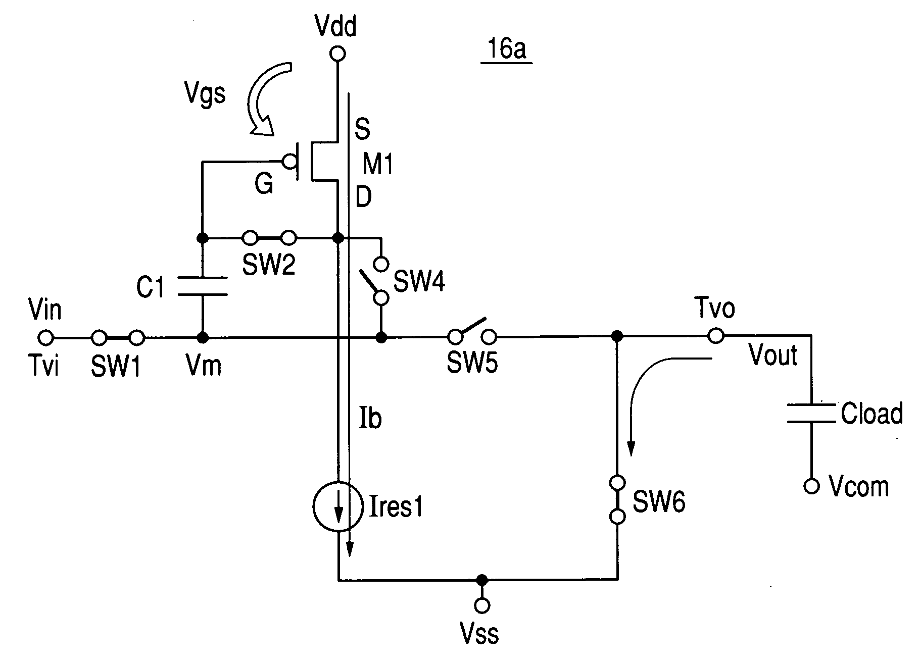
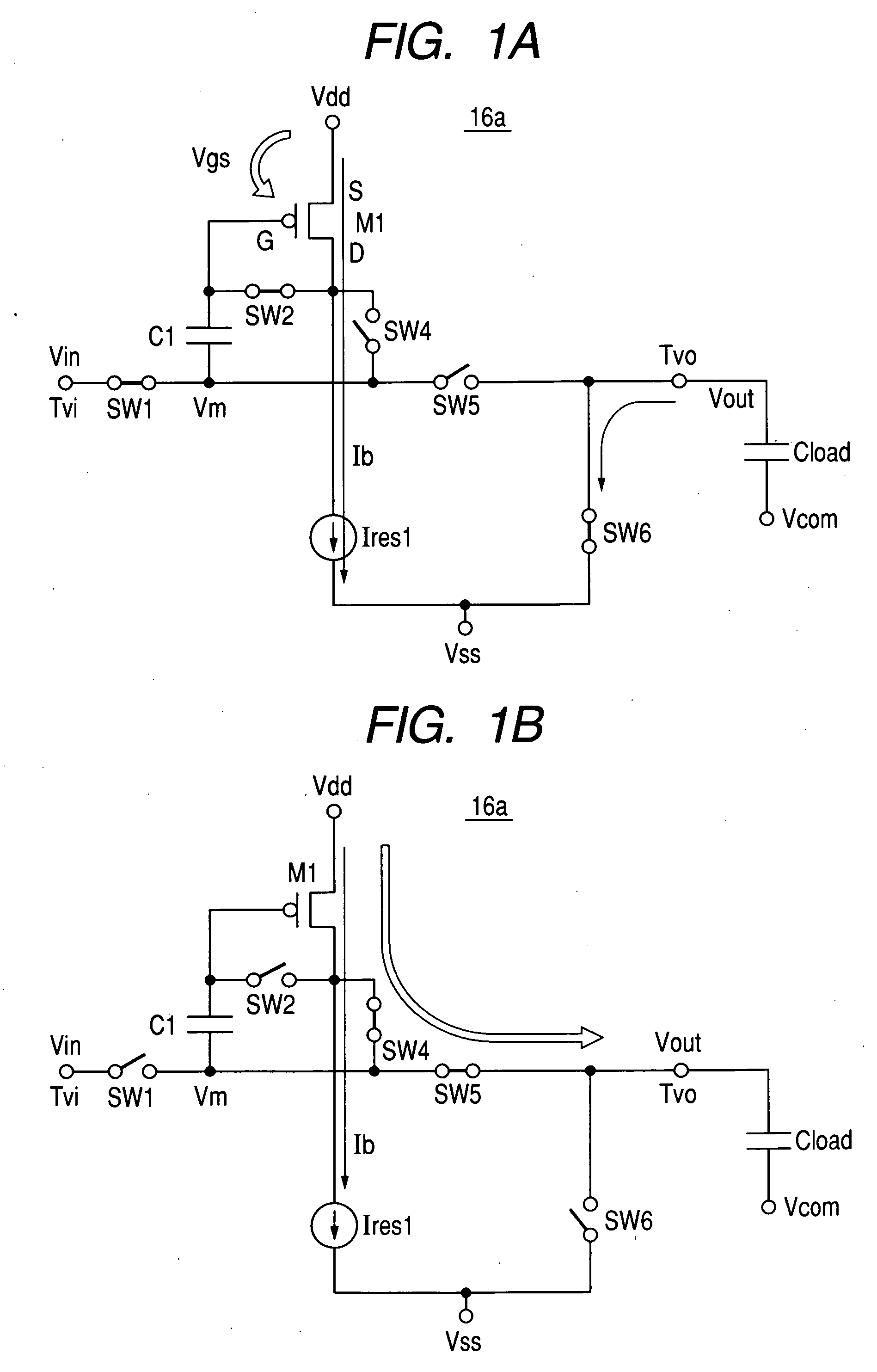
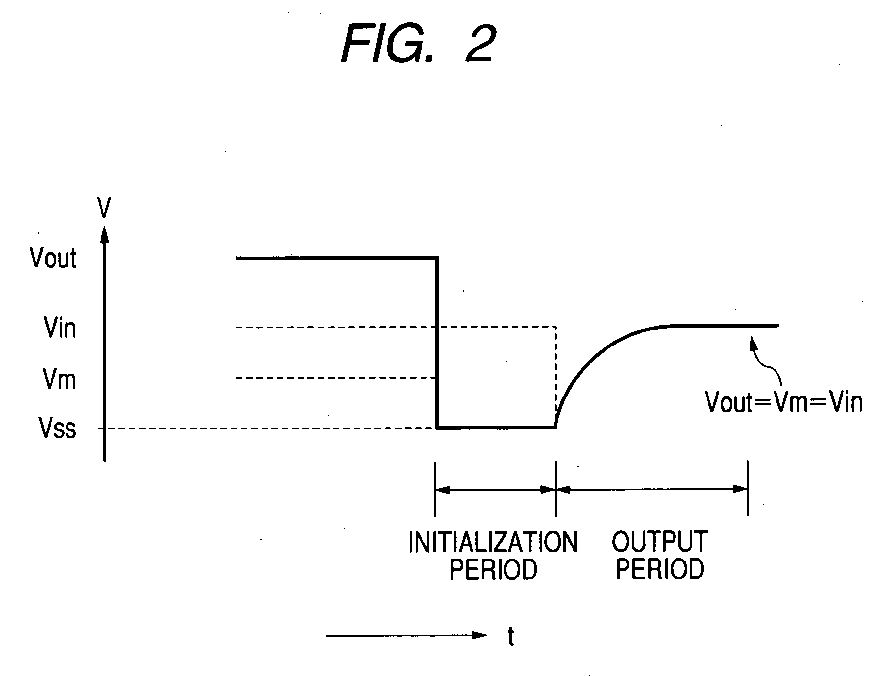
[0037] Hereinafter, preferred embodiments of the present invention will be described with reference to the accompanying drawings. FIG. 1A is a circuit diagram illustrating the configuration of a load capacity driving circuit 16a in accordance with the present invention. Referring to this Figure, the load capacity driving circuit 16a is composed of a pMOS transistor M1 (an amplifying element), a constant current source Ires1 (a constant current circuit) of supplying a constant current having a value Ib, an input capacitor C1 (capacitor), switches SW1, SW2, and SW6 (hereinafter, referred to as first switching means) opened and closed at the same time, and switches SW4 and SW5 (hereinafter, referred to as second switching means). Each of the above-described switches is composed of an analog switch and is opened or closed by a switch control circuit (a control circuit), which is not shown in the figure. The input capacitor C1 preferably has a capacitance of about 0.5 pF to 1 pF. The rea...

second embodiment

[0051] Next, the present invention will be described.

[0052] In the first embodiment, the pMOS transistor M1, serving as a driving transistor, has only a function of supplying a current, so that the load capacitor Cload must be first set to Vss during the initialization period, which causes electric charges to be excessively discharged from the load capacitor Cload, so that power is unnecessarily consumed. This problem is settled by the second embodiment.

[0053] A load capacity driving circuit 16b of the second embodiment operates by repeatedly performing two states, such as the initialization period and the output period, similar to the load capacity driving circuit 16a, and outputs the output voltage Vout resulted from the input voltage Vin with those two periods being used as one period.

[0054]FIG. 3A is a circuit diagram illustrating the configuration of the load capacity driving circuit 16b and the connection states of switch groups during the initialization period in accordance...

third embodiment

[0067] Next, the present invention will be described.

[0068] In the third embodiment, the load capacity driving circuit 16a or 16b according to the first or second embodiment is subjected to an application to constitute a liquid crystal driving circuit for, driving a liquid crystal panel.

[0069]FIG. 5 is a circuit diagram illustrating the configuration of the liquid crystal driving circuit in accordance with the third embodiment of the present invention. Referring to FIG. 5, the liquid crystal driving circuit includes scanning lines 1, data lines 2, thin film transistors (TFTs) 3, pixel electrodes 4 (liquid crystal display pixels), a TFT array 5 constituted of a counter electrode (not shown) with liquid crystal interposed therebetween, a timing controller 9, a scanning line driver 10 (scanning line driving circuit), and a data line driver 11.

[0070] The data line driver 11 is composed of a shift register data latch 12 (storage circuit), an R-string (resistance string) 13, a D / A conve...


PUM

PropertyMeasurementUnit
poweraaaaaaaaaa
capacitanceaaaaaaaaaa
offset voltageaaaaaaaaaa

Abstract

The present invention provides a load capacity driving circuit capable of implementing low power consumption. Switches become closed in an initialization period, and a constant current source allows a bias current to flow through a drain of a MOS transistor, which causes a voltage determined by the current to be generated between a source and a gate thereof. A differential voltage between the potential of the gate of the MOS transistor and an input voltage is stored in a capacitor, and a load capacitor is connected to Vss to be discharged. In a subsequent output period, the switches become open, and switches become closed. Then, the capacitor is connected to the load capacitor, and the MOS transistor is turned on due to a decrease in the potential of the gate, so that the load capacitor is charged until the potential of the gate is restored.

Description

BACKGROUND OF THE INVENTION [0001] 1. Field of the Invention [0002] The present invention relates to an analog buffer circuit and a liquid crystal driving circuit having low power consumption, and particularly, to a load capacity driving circuit suitably used for an output end of a source driver of a liquid crystal driving circuit and to a liquid crystal driving circuit using the same. [0003] 2. Description of the Related Art [0004] In the related art, as shown in FIG. 6, a circuit using an operational amplifier disclosed in Japanese Unexamined Patent Application Publication No. 2000-338461 is used, for example, as a general load capacity driving circuit for driving a capacitive load, such as a liquid crystal panel. This circuit is composed of pMOS transistors P1 to P3, nMOS transistors N1 and N2, constant current sources I1 and I2, and a capacitor Cc. The pMOS transistors P1 and P2, the nMOS transistors N1 and N2, and the constant current source I1 constitute an input end of the op...

Claims


Application Information

Patent Timeline
Patent Type & Authority Applications(United States)
IPC IPC(8): G09G3/20G02F1/133G09G3/36
CPCG09G3/3688G09G2330/021G09G2310/0251A63B43/06F21V33/008
Inventor FUJIYOSHI, TATSUMI
Owner ALPS ALPINE CO LTD
Why Eureka
Try Eureka