Method to prevent passivation layer peeling in a solder bump formation process

a technology of passivation layer and solder bump, which is applied in the direction of semiconductor devices, semiconductor/solid-state device details, coatings, etc., can solve the problems of reducing the yield affecting the reliability of the process, and the tendency of the polymer layer b>14/b> to become detached and peel, so as to improve the yield of the process. the effect of improving the reliability

Inactive Publication Date: 2005-09-01
TAIWAN SEMICON MFG CO LTD
View PDF2 Cites 34 Cited by
  • Summary
  • Abstract
  • Description
  • Claims
  • Application Information

AI Technical Summary

Benefits of technology

[0007] an improved solder bump formation process whereby peeling of passivation layer is avoided to improve a process wafer yield and

Problems solved by technology

Packaging of the ULSI chip is one of the most important steps in ULSI manufacturing, contributing significantly to the overall cost, performance and reliability of the packaged chip.
Packaging of the chip accounts for a considerable portion of the cost of producing the device and failure of the package leads to costly yield reduction.
One of the major problems leading to package failure in UBM formation are caused by the requirement for high temperature thermal treatments and compatibility of materials to withstand high temperature thermal treatments, for example during a curing or a solder reflow process.
For exa

Method used


Image

  • Method to prevent passivation layer peeling in a solder bump formation process
  • Method to prevent passivation layer peeling in a solder bump formation process
  • Method to prevent passivation layer peeling in a solder bump formation process

Examples


Embodiment Construction

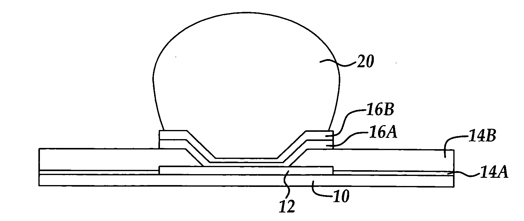
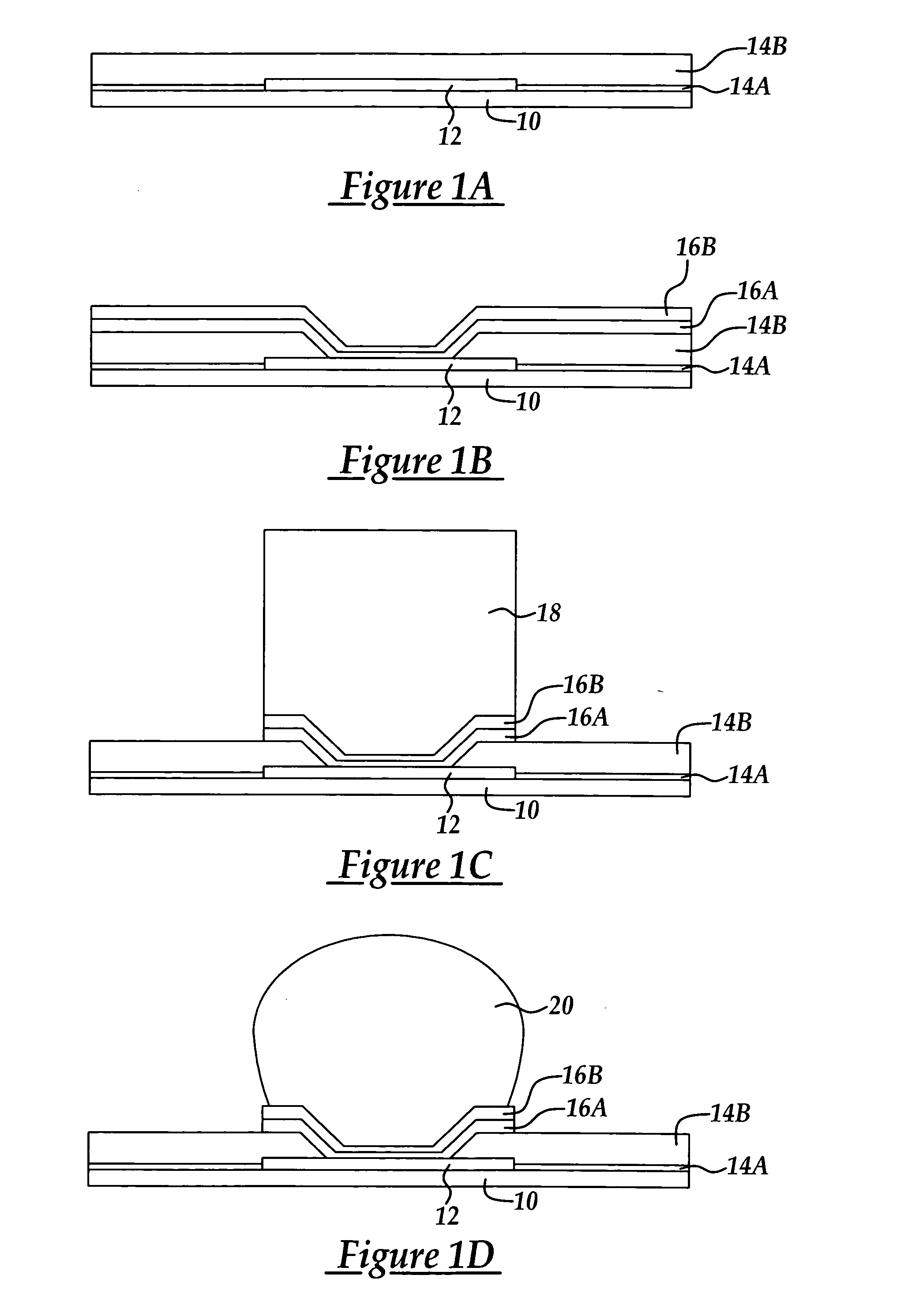
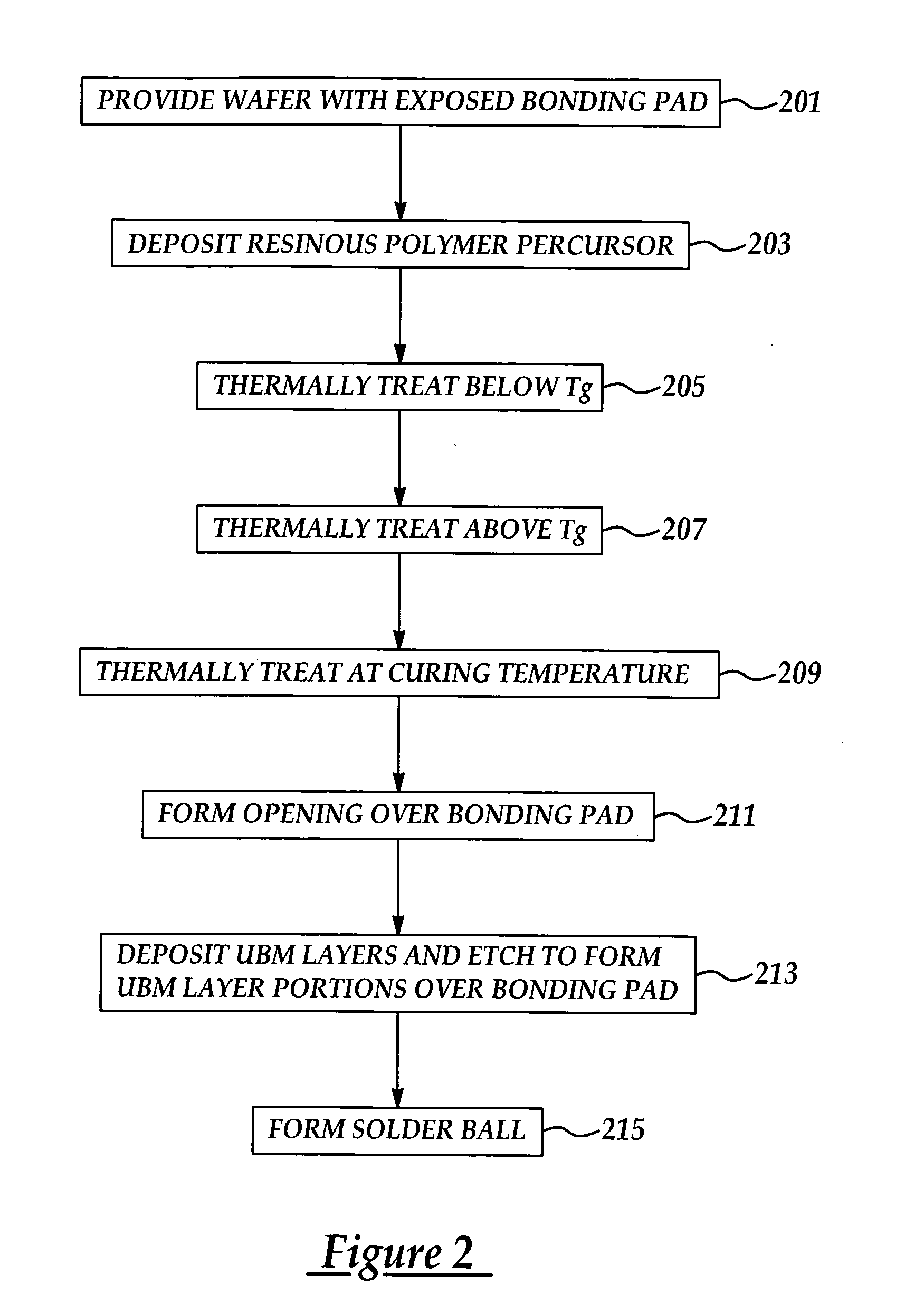
[0013] Although the method of the present invention is explained with reference to a solder bump formation process where a polyimide passivation layer is included as the uppermost passivation layer underlying a UBM system, it will be appreciated that other curable polymer resins producing a cross-linked polymer structure upon exposure to thermal energy and where gaseous species are generated in a curing (energy exposure) process at a temperature above a glass transition temperature (Tg) may also be used as the upper most passivation layer in the method of the present invention. The method of the present invention advantageously avoids the formation of gas pockets or bubbles generated during the curing process above Tg to improve a wafer yield and device reliability in a semiconductor micro-integrated circuit manufacturing process including a solder bump formation process.

[0014] Referring to FIGS. 1A-1D are representative cross-sectional views at stages in a manufacturing process ac...


PUM

PropertyMeasurementUnit
Temperatureaaaaaaaaaa

Abstract

A method for reducing peeling of a cross-linked polymer passivation layer in a solder bump formation process including providing a multi-level semiconductor device formed on a semiconductor process wafer having an uppermost surface comprising a metal bonding pad in electrical communication with underlying device levels; forming a layer of resinous pre-cursor polymeric material over the process surface said resinous polymeric material having a glass transition temperature (Tg) upon curing; subjecting the semiconductor process wafer to a pre-curing thermal treatment temperature below Tg for a period of time; and, subjecting the semiconductor process wafer to at least one subsequent thermal treatment temperature above Tg for a period of time to form an uppermost passivation layer.

Description

FIELD OF THE INVENTION [0001] This invention generally relates to semiconductor processing including under bump metallurgy (UBM) formation in flip chip bonding technology and more particularly to formation of a polymer passivation layer to avoid gas bubble formation and subsequent peeling in a solder bump formation process. BACKGROUND OF THE INVENTION [0002] Packaging of the ULSI chip is one of the most important steps in ULSI manufacturing, contributing significantly to the overall cost, performance and reliability of the packaged chip. As semiconductor devices reach higher levels of integration, packaging technologies such as chip bonding have become critical. Packaging of the chip accounts for a considerable portion of the cost of producing the device and failure of the package leads to costly yield reduction. [0003] One of the major problems leading to package failure in UBM formation are caused by the requirement for high temperature thermal treatments and compatibility of mate...

Claims


Application Information

Patent Timeline
IPC IPC(8): C08J7/04H01L21/44H01L21/60H01L21/768
CPCH01L24/11H01L2224/0401H01L2224/13099H01L2924/01013H01L2924/01022H01L2924/01029Y10S438/907H01L2924/14H01L2924/01006H01L2924/01024H01L2924/01033H01L2924/014H01L2924/01082H01L2224/05124H01L2224/05147H01L2224/05155H01L2224/05166H01L2224/05171H01L2224/05647H01L2224/05655H01L2224/05671H01L21/56H01L24/13H01L24/05H01L24/03H01L23/3157H01L2224/131H01L2924/00014H01L2924/013H01L2924/01023
Inventor TZENG, KAIWU, CHENG-MINGHU, CHU-WEIHSU, JUNG-LIEHHSU, KUEI-YUAM
Owner TAIWAN SEMICON MFG CO LTD
Why Eureka
Try Eureka