
Simulation apparatus and method of designing semiconductor integrated circuit

a technology of integrated circuits and simulation apparatuses, applied in the direction of instruments, analogue processes for specific applications, electric/magnetic computing, etc., can solve the problems of limited battery life, inability to carry out simulation, and insufficient simulation time, etc., to achieve low power consumption and high precision design

Inactive Publication Date: 2005-09-01
PANASONIC CORP
View PDF3 Cites 21 Cited by
  • Summary
  • Abstract
  • Description
  • Claims
  • Application Information

AI Technical Summary

Benefits of technology

[0010] An object of the present invention is to provide a power consumption estimating method in a high speed and in high precision, while a simulation model designing method is realized and this simulation model is employed. That is, in a simulation apparatus of a semiconductor integrated circuit, such a simulation model designing method is realized which is capable of executing a simulation in a high speed and in a higher abstract degree than the RT level by employing a general-purpose programming language such as the C language, in cooperation with installed software and the like. Another object of the present invention is to provide a low power consumption designing method capable of realizing low power consumption by employing this estimated result in a floor plan step and an arranging / wiring step, while suppressing a simulation-returning-back process operation in a minimum value.
[0029] Also, in accordance with the power consumption estimating method of present invention, the power consumption can be estimated in high precision, namely, ±20% of the actual measurement value before the correction is made, and ±10% of the actual measurement value after the correction is made. Furthermore, in accordance with the low power consumption designing method of the present invention, while the simulation-returning-back process operation is suppressed to the minimum value within the floor plan step and the arranging / wiring step, the low power consumption designing can be realized.

Problems solved by technology

In particular, as to semiconductor integrated circuits used in portable terminals, utilization fields of these portable terminals are expanded to multimedia fields, for instance, Internet connections, TV telephones, reproductions of moving pictures under such a condition that lifetimes of batteries thereof are limited.
However, in order to estimate power consumption by using the RT level, the net list, and arranging / wiring information, a plenty of simulation time is necessarily required.
Thus, there are some events that such a simulation cannot be carried out, depending upon scales of LSIs.
Also, while short-term development of LSIs has been requested, there are some events that such processing steps used to estimate power consumption cannot be secured.
Furthermore, since a database used to predict areas and energy data per unit area are provided, power consumption is predicted.
In the former technique, since the transaction analyzed results are statistically processed, errors from the actual operations become large.
However, the later technique owns the following problem.
There is another problem that a simulation-returning-back process operation is increased in such a case that a specification cannot be satisfied while power consumption is predicted.

Method used


Image

  • Simulation apparatus and method of designing semiconductor integrated circuit
  • Simulation apparatus and method of designing semiconductor integrated circuit
  • Simulation apparatus and method of designing semiconductor integrated circuit

Examples


embodiment mode 1

[0051] Best embodiment modes of the present invention will now be explained in detail with reference to drawings. First, a description is made of a simulation model designing method having a high abstract degree and capable of realizing a high speed cycle base simulation, which corresponds to a first object of the present invention.

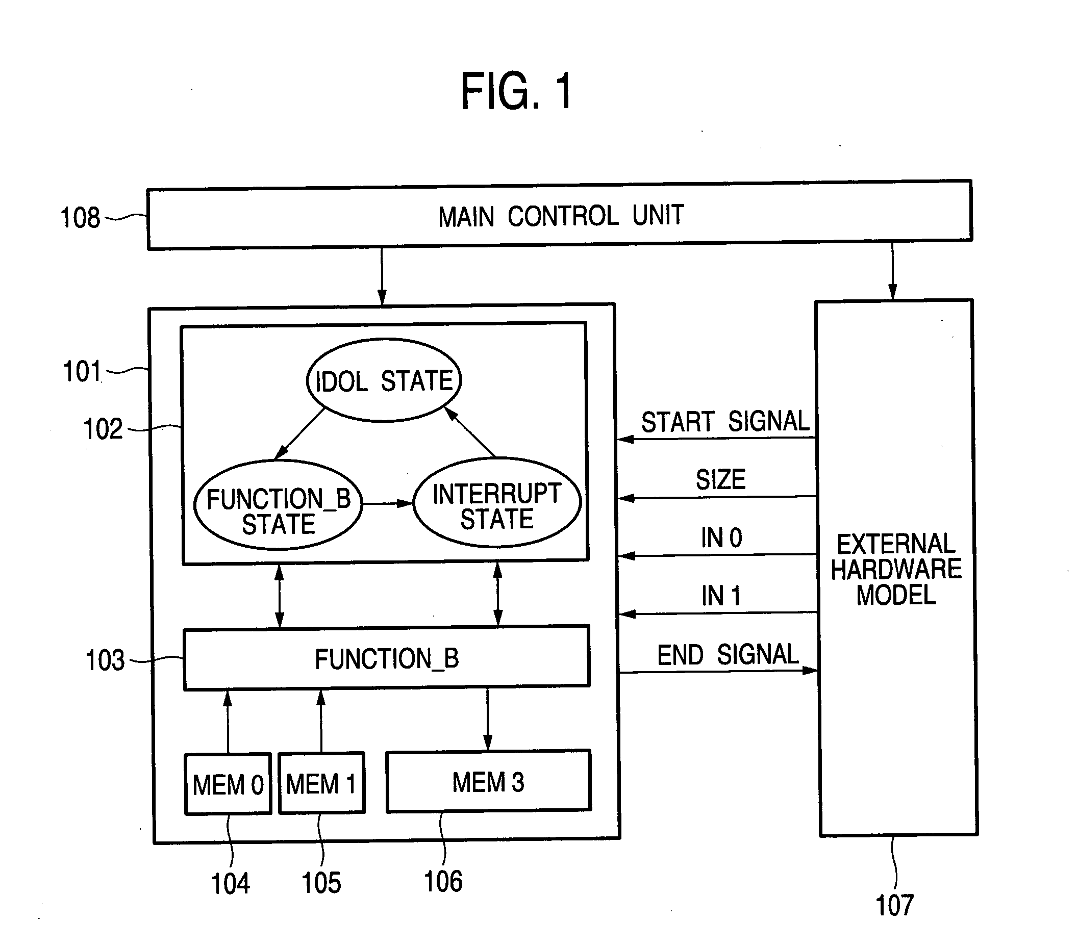
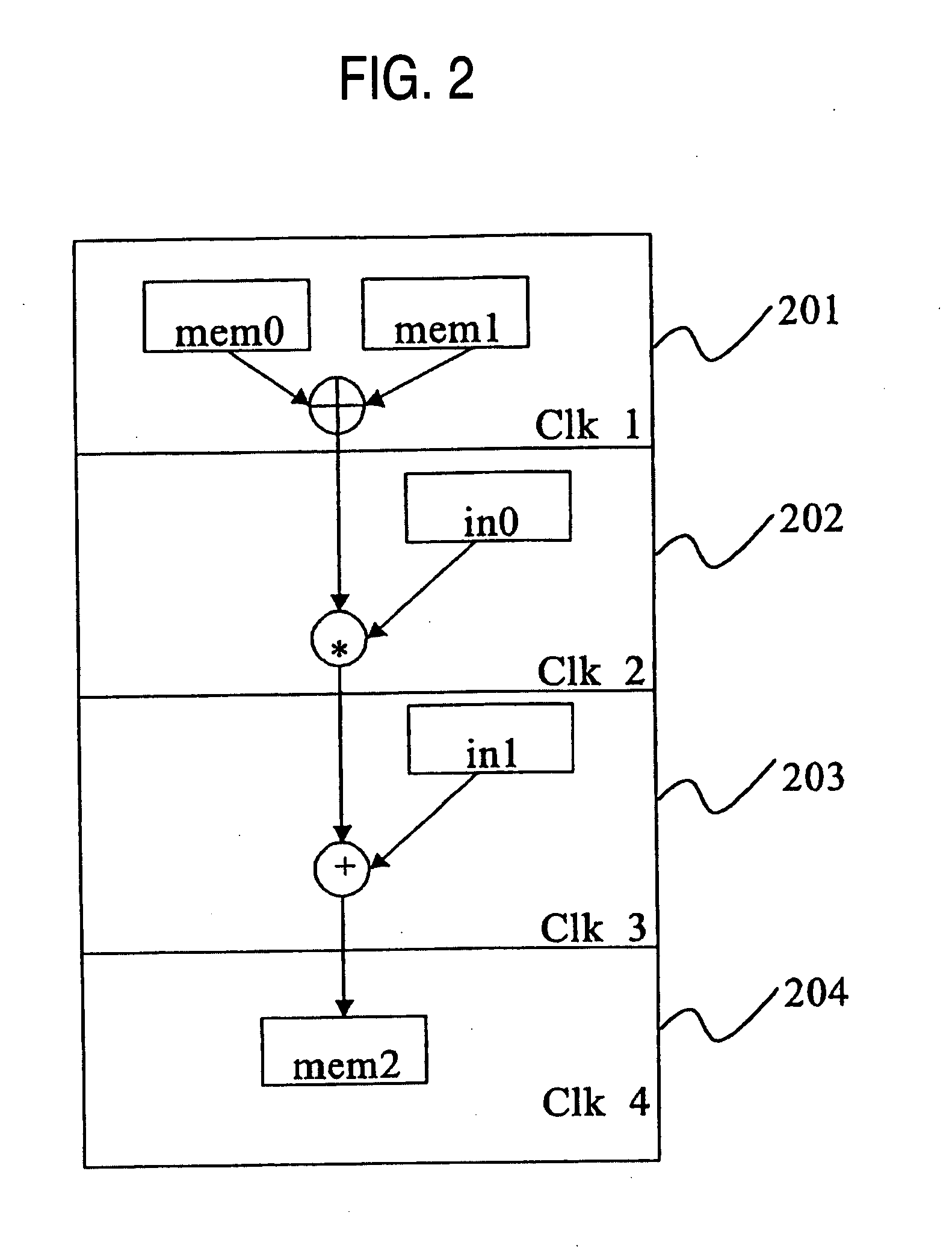
[0052] To this end, “function_b” is indicated as an algorithm model example of hardware which has been described by using a C language as follows:

void function_b(size_a,in0,in1){int i, tmp;for(i=0;itmp = mem0[i]+ mem1[i];tmp *= in0;tmp += in1;mem2[i] = tmp;}}

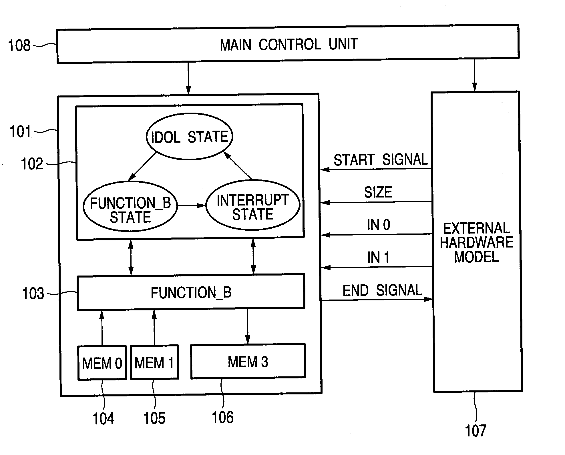
[0053]FIG. 1 is a schematic diagram for showing a simulation apparatus equipped with the high-speed cycle base model, according to the present invention, which corresponds to this algorithm model. A model 101 to be desingned is arranged by a state control module model 102, a calculation module model 103, and memory models 104, 105, 106. Also, there are a “start_signalsignal for notifying a start ...

embodiment mode 2

[0064] A description is made of a method for estimating power consumption in high precision from a simulation model of a high abstract degree, which corresponds to a second object of the present invention, with reference to the hardware model of the embodiment mode 1. FIG. 4 is a schematic diagram for indicating a simulation apparatus equipped with a power consumption measuring function. While software and the like which have been installed in this simulation apparatus are utilized, a simulation of an actual operation is executed so as to perform a power consumption measuring operation, so that an estimation of a power consumption value is obtained.

[0065] In this simulation apparatus, every time a certain constant section (T) set via a user interface 402 is elapsed, both an operation cycle number (Act) of the calculation module model 103 and access numbers (Actmem) of the memory models 104, 105, 106 are measured by the power measuring unit 401. The calculation module model 103 is u...

embodiment mode 3

[0070] A description is made of a low power consumption designing method in both a floor plan step and an arranging / wiring step with employment of a power consumption estimation result obtained from a simulation model with a high abstract degree, which corresponds to a third object of the present invention. FIG. 5 is a flow chart for describing a low power consumption designing method of a semiconductor integrated circuit, according to an embodiment mode 3 of the present invention, while this low power consumption designing method is made based upon both the simulation model designing method of the embodiment mode 1 and the power consumption estimating method of the embodiment mode 2.

[0071] In FIG. 5, first of all, in an architecture design step ST1, both partitioning and detailed specifications as to both hardware and software are designed, and both a hardware model D1 of an algorithm description and a software model D2 of a C program are formed.

[0072] Next, based upon the simula...


PUM


Abstract

A simulation apparatus of a semiconductor integrated circuit, capable of measuring power consumption in a higher abstract degree than an RT level and in a high speed, is realized, so that a low power consumption designing operation can be carried out by employing a simulation result. While a cycle base model of a designing subject circuit is arranged by a state control module model, a calculation module model, and a memory model, in the calculation module model, an algorithm description is made; a detailed structure such as a pipeline of hardware is shortcircuited to a calculation to be processed in a unit clock; and a timing shift is absorbed in a wait state of the state control module model, so that a high-speed simulation can be realized. Since such information as an area and a wiring capacitance is added to an activating ratio measurement of a simulation model, power consumption can be measured. A priority arraigning / wiring operation of a function module is carried out based upon this measurement result, and then, a simulation is repeatedly performed so as to execute optimum arranging / wiring operations, so that low power consumption designing can be realized.

Description

BACKGROUND OF THE INVENTION [0001] 1. Field of the Invention [0002] The present invention is related to a method of designing a system LSI. More specifically, the present invention is directed to a simulation model designing method in a simulation apparatus of an LSI, a power consumption estimating method using this model, and also, directed to a low power consumption designing method in a layout step and an arranging / wiring step based upon this estimated result. [0003] 2. Description of the Related Art [0004] Very recently, in semiconductor integrated circuits such as system LSIs which have been manufactured in large scales, reductions of power consumption are strongly required. In particular, as to semiconductor integrated circuits used in portable terminals, utilization fields of these portable terminals are expanded to multimedia fields, for instance, Internet connections, TV telephones, reproductions of moving pictures under such a condition that lifetimes of batteries thereof ...

Claims


Application Information

Patent Timeline
Patent Type & Authority Applications(United States)
IPC IPC(8): G06F17/50H01L21/82
CPCG06F17/5022G06F30/33
Inventor KUWAHARA, YUJISHINDE, HIROKIOGAWA, SACHIO
Owner PANASONIC CORP
Learn More