Nitride semiconductor device and method of manufacturing the same

a semiconductor and nitride technology, applied in the field of semiconductor devices, can solve the problems of low optical efficiency, low yield, high cost of production, etc., and achieve the effect of high optical efficiency

Active Publication Date: 2005-09-15
LG SILTRON +1
View PDF2 Cites 79 Cited by
  • Summary
  • Abstract
  • Description
  • Claims
  • Application Information

AI Technical Summary

Benefits of technology

[0006] The present invention provides a nitride semiconductor device having high optical efficiency.
[0007] The present invention also provides a method of manufacturing a nitride semiconductor device, which can employ a variety of substrates and deposit a nitride semiconductor thin film having high optical efficiency and good quality on a large-sized substrate.

Problems solved by technology

However, when a light emitting diode is manufactured using the nitride semiconductor thin film grown on the sapphire substrate, it has high internal quantum efficiency (QE), but low optical efficiency (OE) due to optical emission restrictions caused by internal scattering.
Also, in the conventional manufacturing process of nitride semiconductor thin films, since an expensive and small-sized sapphire substrate is used, the resulting nitride semiconductor thin film has a small size of 2 inches or less, the cost of production is high, and yield is low.

Method used


Image

  • Nitride semiconductor device and method of manufacturing the same
  • Nitride semiconductor device and method of manufacturing the same
  • Nitride semiconductor device and method of manufacturing the same

Examples


embodiment

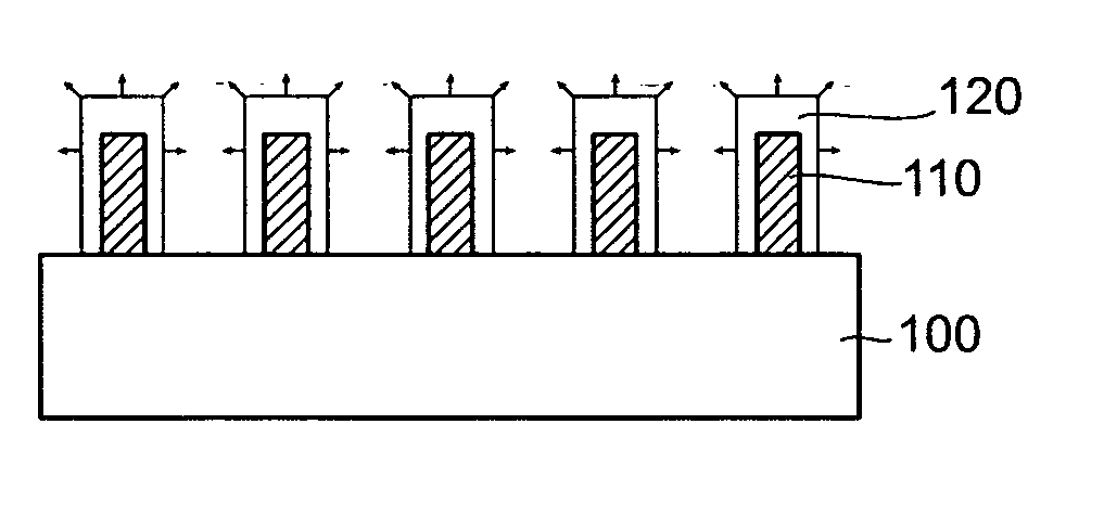
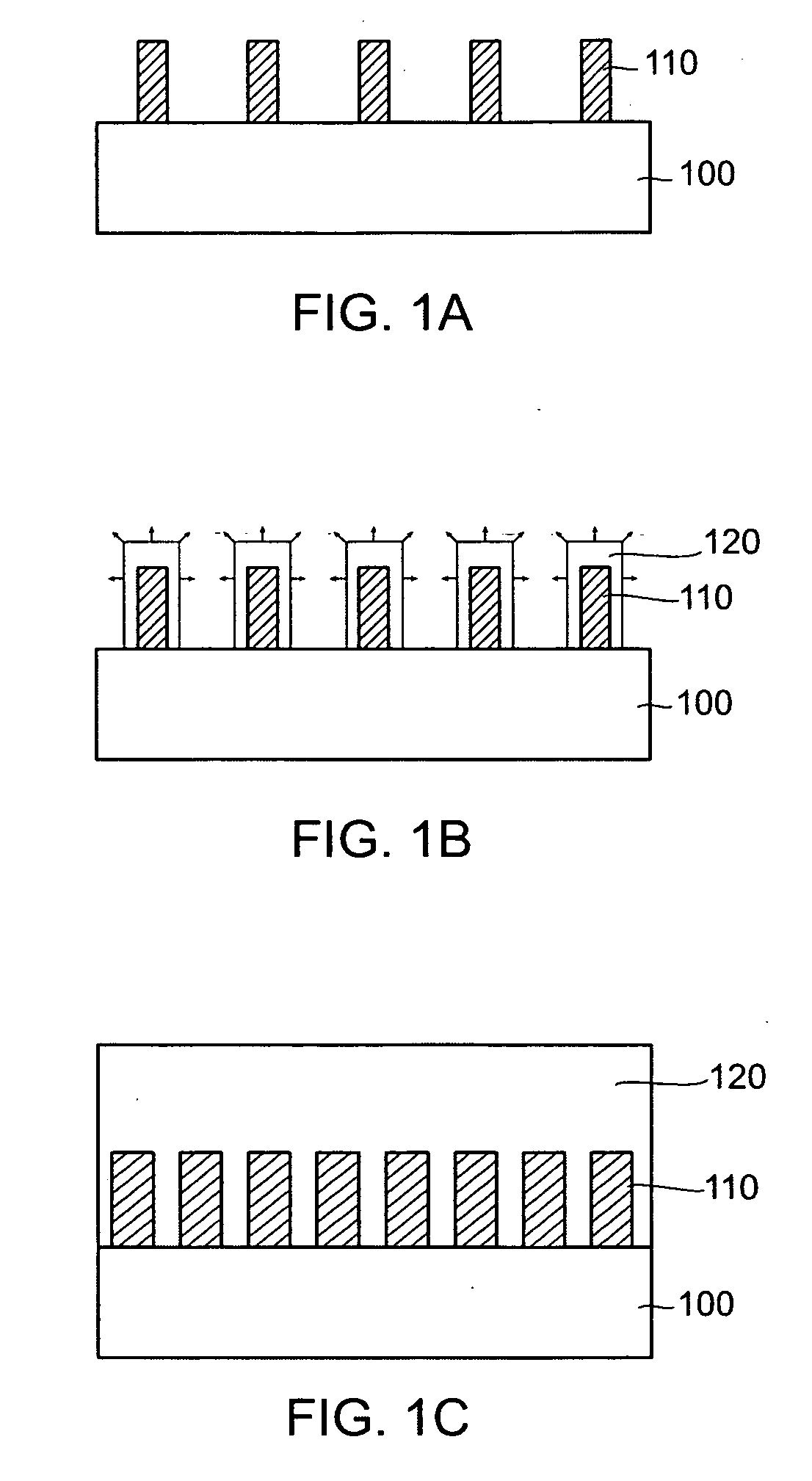
[0037] A process of forming ZnO nanorods will now be described by giving a specific example. At the outset, reactive precursors (i.e., Zn(CH3)2 and O2) were injected through separate lines into a reactor at flow rates of 0.1 to 10 sccm and 10 to 100 sccm, respectively, using Ar as a carrier gas. A chemical reaction between the Zn(CH3)2 and O2 occurred on a silicon substrate, thus growing ZnO nanorods in a vertical direction with respect to the plane of the silicon substrate, as shown in FIG. 1A. While the ZnO nanorods are being grown over about 1 hour, the reactor was maintained at a pressure of 10−5 to 760 mmHg and a temperature of 400 to 900° C. After the growth of the ZnO nanorods was finished, each of the ZnO nanorods grown on the silicon substrate had a diameter of about 1 to 1000 nm and a length of about 10 nm to 100 μm.

[0038] A process of forming SiC nanorods will now be described by giving a specific example. At first, a metal catalyst e.g., Au, Ni, or Fe was coated on a su...


PUM

PropertyMeasurementUnit
lengthaaaaaaaaaa
diameteraaaaaaaaaa
temperatureaaaaaaaaaa

Abstract

Provided are a nitride semiconductor device and method of manufacturing the same. In the method, semiconductor nanorods are vertically grown on a substrate, and then a nitride semiconductor thin film is deposited on the substrate having the semiconductor nanorods. Accordingly, a high-quality nitride semiconductor thin film can be deposited on a variety of inexpensive, large-sized substrates. Also, because the nitride semiconductor thin film containing the semiconductor nanorods can easily emit light through openings between the nanorods, internal scattering can be greatly reduced. Thus, the nitride semiconductor thin film can be usefully employed in optical devices such as light emitting diodes and electronic devices.

Description

BACKGROUND OF THE INVENTION [0001] 1. Field of the Invention [0002] The present invention relates to a semiconductor device and a method of manufacturing the same, and more particularly, to a nitride semiconductor device having high optical efficiency and a method of manufacturing the same. [0003] 2. Description of the Related Art [0004] In recent years, owing to increased demand for blue-wavelength light emitting diodes, GaN thin films have become strongly relied upon. As is well known to those skilled in the art, a nitride semiconductor thin film, such as the GaN film, is typically deposited on a sapphire (Al2O3) substrate. [0005] However, when a light emitting diode is manufactured using the nitride semiconductor thin film grown on the sapphire substrate, it has high internal quantum efficiency (QE), but low optical efficiency (OE) due to optical emission restrictions caused by internal scattering. Also, in the conventional manufacturing process of nitride semiconductor thin film...

Claims


Application Information

Patent Timeline
Patent Type & Authority Applications(United States)
IPC IPC(8): C23C16/34C23C16/40H01L21/205H01L27/15H01L29/04H01L29/10H01L29/26H01L31/036H01L31/0376H01L31/12H01L31/20
CPCH01L21/02381H01L21/02439H01L21/02447H01L21/02472H01L21/02513Y10S977/759H01L21/0262H01L21/02645H01L33/007H01L33/12H01L21/0254B82Y40/00H01L21/20
Inventor YI, GYU-CHULAN, SUNG JINKIM, YONG JIN
Owner LG SILTRON
Why Eureka
Try Eureka