Semiconductor element and wafer level chip size package therefor

a technology of semiconductor elements and chip sizes, applied in the direction of semiconductor devices, semiconductor/solid-state device details, electrical apparatus, etc., can solve the problems of not providing space for marking, not equipped with heat dissipation structures allowing efficient, and not providing heat dissipation effects, etc., to avoid the curvature of semiconductor devices, improve heat dissipation characteristics, and increase the overall area of the surfa

Inactive Publication Date: 2005-09-15
YAMAHA CORP
View PDF11 Cites 65 Cited by
  • Summary
  • Abstract
  • Description
  • Claims
  • Application Information

AI Technical Summary

Benefits of technology

[0052] It is an object of the invention to provide a semiconductor device that can be manufactured in the form of the WLCSP and that can efficiently dissipate heat generated by a semiconductor chip to the exterior thereof.
[0053] It is another object of the invention to provide a semiconductor element and a wafer level chip size package therefor, which can improve heat dissipation characteristics without increasing the effective area of the semiconductor element, which is easy to discriminate the direction of the semiconductor element, and which can be processed to present information specifically designated by the semiconductor element.
[0054] It is a further object of the invention to provide a semiconductor element and a board therefor, which can realize downsizing and thickness reduction of a product without increasing the number of parts and manufacturing processes and without increasing the overall height and volume of the product.

Problems solved by technology

Conventionally, WLCSP is not equipped with a heat dissipation structure allowing efficient dissipation of heat generated by a semiconductor chip.
H11-67998, heat dissipation effects can be increased because the overall area is increased due to irregularities formed on the planar surface; however, there still remains a problem due to the limited heat dissipation effects thereof.
The conventional WLCSP has a very narrow surface area, which does not provide space for arranging a marking space thereon.
This causes difficulty for the human operator to discriminate the direction of the semiconductor element.
This makes it very difficult for the manufacturer to reduce the production cycle in manufacturing of semiconductor chips and to reduce the manufacturing cost therefor.
In addition, it is very difficult to downsize manufacturing machines, which causes bottlenecks in reducing the manufacturing cost.
This increases the number of parts and the number of manufacturing processes, which in turn increase the manufacturing cost.
When the permanent magnet 205 and the magnetic materials 209, 214, and 216 are changed in positioning, it is necessary to re-design products, which causes excessive cost in designing.
This causes unwanted limitations against the downsizing and thickness reduction of the product.
This causes error, malfunction, and difficulty in reading with regard to the identification codes 306.
In addition, the WLCSP 304 requires a specially designed machine, i.e., an ink dot laser printer, in order to print the identification codes 306, which is troublesome.
This causes error, malfunction, and difficulty in reading with regard to the identification codes 308.
Due to such a relatively small degree of freedom regarding re-wiring (or re-drawing of wires), the aforementioned structure have difficulty in coping with complicated arrangement of external terminals in LSI devices.
In addition, this limits the total density of external terminals (i.e., the number of external terminals per unit area).
However, this may greatly push up the manufacturing cost, which is inconvenient for manufacturers.
However, the reduction of the terminal base causes a reduction of the joining strength of the external terminal, whereby the semiconductor device should be degraded in reliability.
In addition, ‘spherical’ metal posts may be easily destructed or easily separated off from the semiconductor chip.
Due to the formation of the V-shaped channel portions 506 on the surface and backside of the base substrate 502, the CSP 501 is disadvantageous in that the base substrate 502 is slightly reduced in rigidity and the end portions thereof may be easily deformed.
However, it is very difficult to avoid the occurrence of the entire curvature of the CSP 501 including the semiconductor chip 503.

Method used


Image

  • Semiconductor element and wafer level chip size package therefor
  • Semiconductor element and wafer level chip size package therefor
  • Semiconductor element and wafer level chip size package therefor

Examples


first embodiment

1. First Embodiment

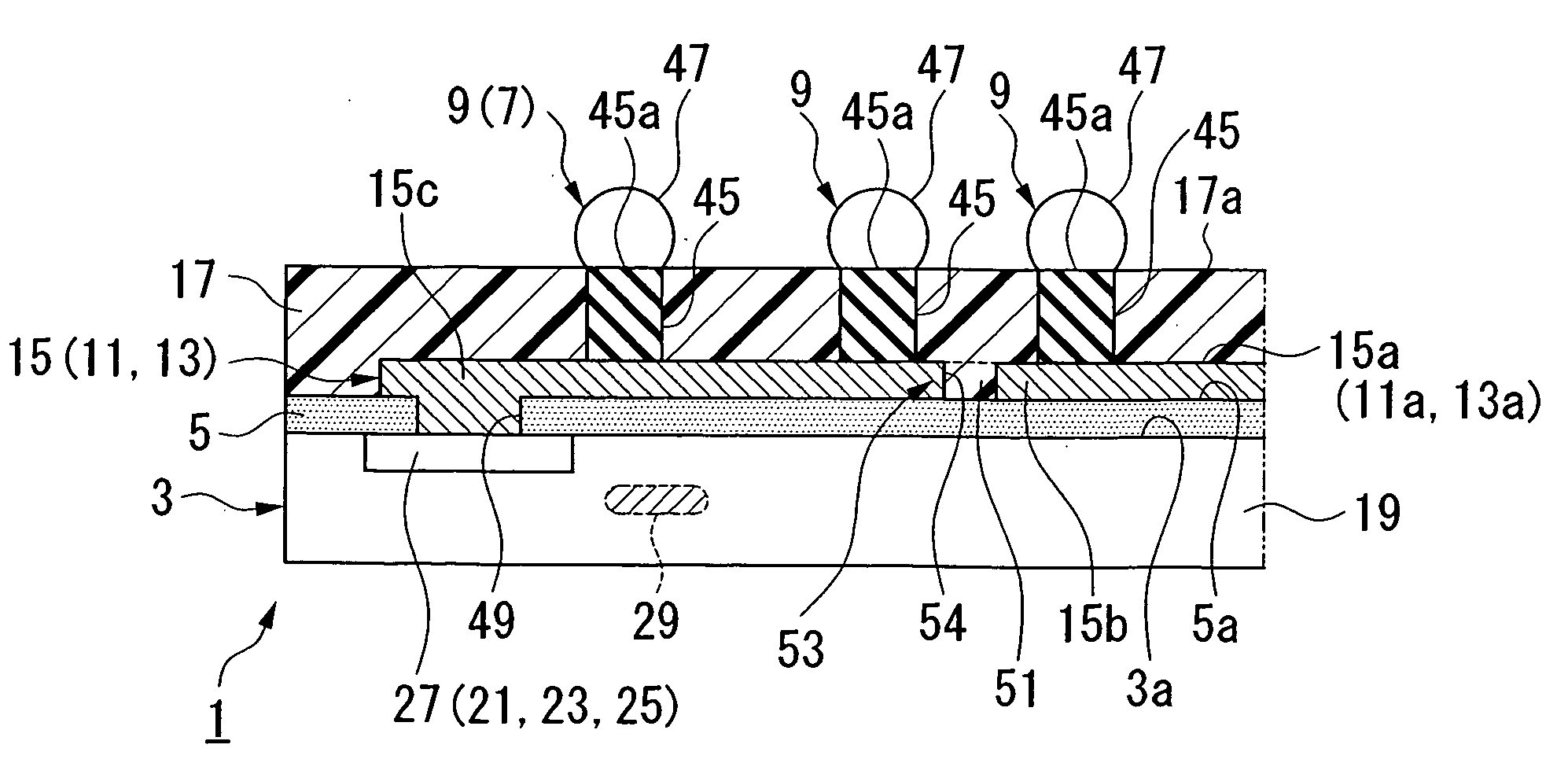
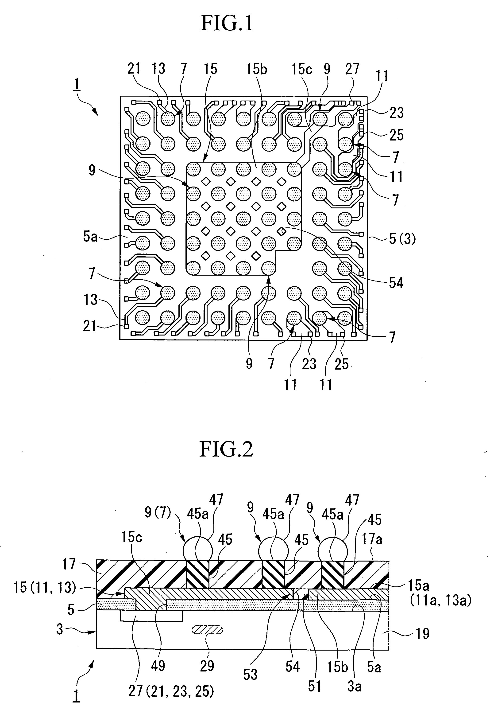
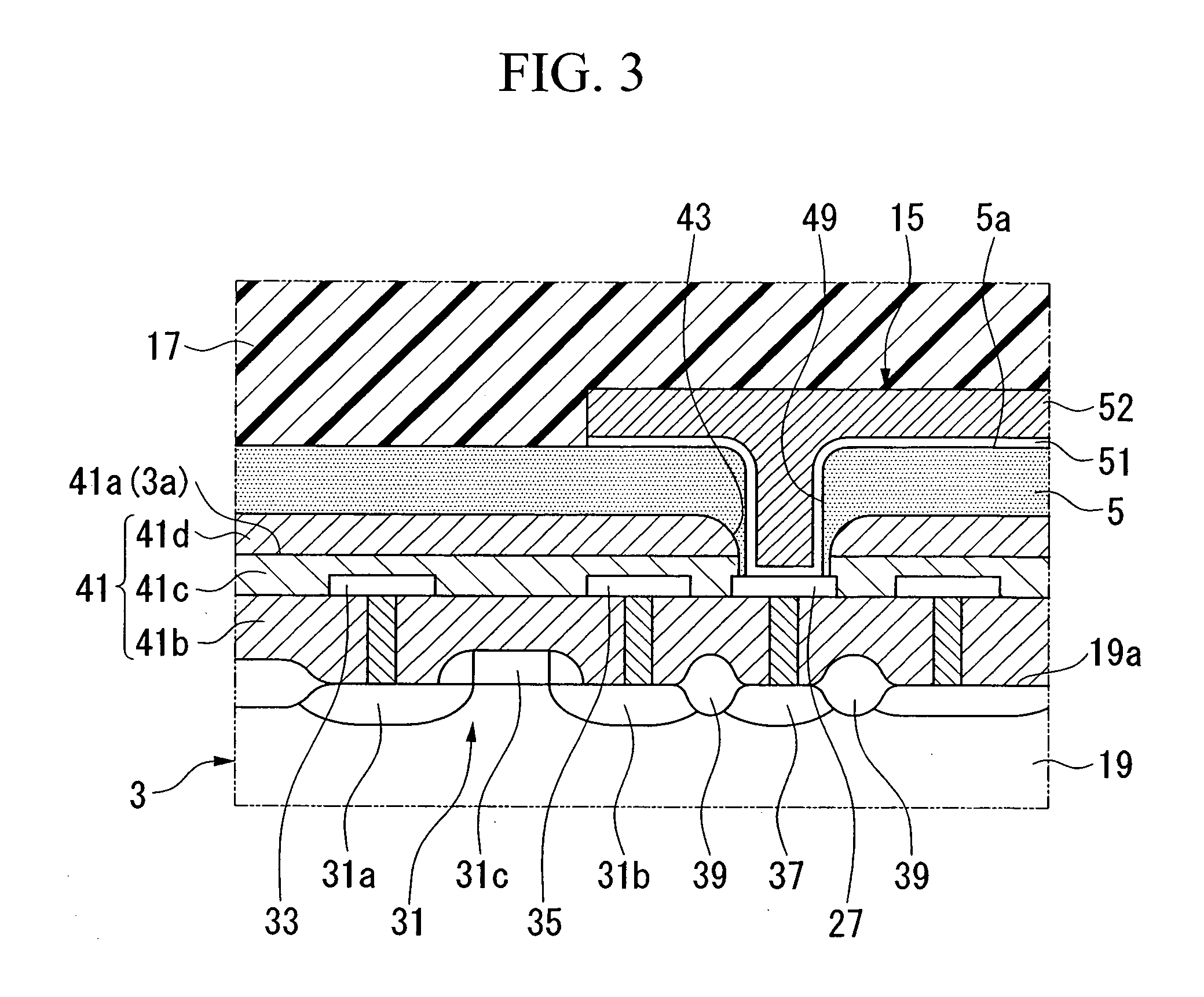
[0167] A semiconductor device according to a first embodiment of the invention will be described with reference to FIGS. 1, 2, 3, 4A-4F, and 5. As shown in FIGS. 1 and 2, a semiconductor device 1 includes a semiconductor chip 3 having a rectangular plate-like shape in plan view, an insulating layer 5 (serving as a first insulating layer) formed on a surface 3a of the semiconductor chip 3, a plurality of connection electrodes 7 and heat-dissipation electrodes 9 arranged on the surface 3a of the semiconductor chip 3, a plurality of wiring portions 11, 13, and 15 that are formed on a surface Sa of the insulating layer 5 so as to establish mutual connections between the semiconductor chip 3 and the connection electrodes 7 or the heat-dissipation electrodes 9, and a molded resin 17 (serving as a second insulating layer), which covers the surface 5a of the insulating layer 5 in such a condition that the electrodes 7 and 9 are exposed to the surface 3a of the semiconduct...

second embodiment

2. Second Embodiment

[0218]FIG. 16 is a perspective view showing the exterior appearance of a wafer level chip size package (WLCSP) in accordance with a second embodiment of the invention. FIG. 17 is a front view of the WLSCP; and FIG. 18 is a side view of the WLCSP. Reference numeral 101 designates a silicon substrate (or a semiconductor substrate) having a rectangular shape in plan view, on which integrated circuits (or electronic circuits, not shown) are formed. Reference numerals 102 designate metal pads realizing connections with external devices, which are arranged in a rectangular formation along the peripheral portion of a prescribed surface 101a of the silicon substrate 101 and each of which has a semi-elliptical shape in cross section. Reference numerals 103 designate channels, which are formed in parallel with each other on a backside surface 101b opposite to the prescribed surface 101a and each of which has a rectangular shape in cross section. As shown in FIG. 17, the ch...

third embodiment

3. Third Embodiment

[0264]FIG. 26 is a side view showing a wafer level chip size package (WLCSP) that is mounted on a printed-circuit board in accordance with a third embodiment of the invention; FIG. 27 is a plan view showing a prescribed surface of the WLCSP; and FIG. 28 is a plan view showing a prescribed surface of the printed-circuit board.

[0265] A WLCSP 221 includes a silicon substrate (or a semiconductor substrate) 222 having a rectangular shape in plan view, in which integrated circuits (or electronic circuits, not shown) are formed. Connection pins (serving as first terminals) 223, which are composed of conductive materials such as copper (Cu) and aluminum (Al) so as to establish electric connections with external devices, are arranged at selected points of the grid on a prescribed surface 222a of the silicon substrate 222. Non-connection pins (serving as second terminals) 224, which are not electrically connected with external devices, are arranged at other selected positi...


PUM


Abstract

A semiconductor device, encapsulated in a wafer level chip size package (WLCSP), includes a plurality of pad electrodes formed on the surface of a semiconductor chip, wherein a first insulating layer is formed on the surface of the semiconductor chip except the pad electrodes; a plurality of connection electrodes and at least one heat-dissipation electrode are formed on the surface of the first insulating layer; the pad electrodes and the connection electrodes are mutually connected via a first wiring portion; the heat-dissipation electrode is connected with a second wiring portion; and a second insulating layer is formed to enclose the electrodes and wiring portions, wherein the second wiring portion is arranged in proximity to a heating portion of the semiconductor chip and is formed on the surface of the first insulating layer except the prescribed region corresponding to the first wiring portion.

Description

BACKGROUND OF THE INVENTION [0001] 1. Field of the Invention [0002] This invention relates to semiconductor elements and wafer level chip size packages (WLCSP) therefor. [0003] This application claims priority on Japanese Patent Applications Nos. 2004-158984, 2004-72375, 2004-80837, 2004-175262, 2004-173986, and 2004-351806, the contents of which are incorporated herein by reference. [0004] 2. Description of the Related Art [0005] In semiconductor devices such as LSI devices, integrated circuits such as transistors and various electronic components are formed on surfaces of semiconductor chips, which thus generate heat when operated. In order to avoid error and malfunction due to excessive heat generated in semiconductor chips, various heatsink structures and heat dissipation structures for effectively dissipating heat from semiconductor devices have been developed. For example, Japanese Patent Application Publication No. 2002-158310 teaches a semiconductor device equipped with a he...

Claims


Application Information

Patent Timeline
Patent Type & Authority Applications(United States)
IPC IPC(8): H01L23/12H01L23/34H01L23/48H01L23/50H01L23/52
CPCH01L23/12H01L2924/10158H01L23/48H01L23/50H01L23/52H01L2924/01066H01L2924/01067H01L2924/01068H01L2924/01322H01L23/34H01L24/17H01L2224/14132H01L2224/16238H01L2224/131H01L2224/13023H01L2224/13022H01L2224/05571H01L2224/8113H01L2224/81132H01L2224/81122H01L2224/05569H01L2224/02377H01L2224/05548H01L2224/05556H01L2924/00H01L2924/014H01L2924/00012H01L2924/351H01L2924/181H01L2924/12042H01L2224/0401H01L2224/05559H01L2924/14H01L2924/00011H01L2224/13H01L2224/05124H01L2224/05147H01L2224/05166H01L2224/05171H01L2224/05624H01L2224/05647H01L2224/06131H01L2224/0615H01L24/05H01L2223/54406H01L23/3114H01L23/544H01L2223/54433H01L2224/81805H01L2924/00014
Inventor NOMOTO, KENTAROIGAWA, YUKISAITOH, HIROSHISATO, TAKASHIOHASHI, TOSHIOOHKURA, YOSHIHIRO
Owner YAMAHA CORP
Why Eureka
Try Eureka