

Semiconductor chip and fabrication method thereof
a semiconductor chip and semiconductor technology, applied in semiconductor devices, semiconductor/solid-state device details, electrical devices, etc., can solve the problems of affecting the formation of high-density semiconductor chips on semiconductor wafers
- Summary
- Abstract
- Description
- Claims
- Application Information
AI Technical Summary
Benefits of technology
Problems solved by technology
Method used
Image

Examples
Embodiment Construction
[0029] In the following, embodiments of the present invention will be described with reference to the accompanying drawings.
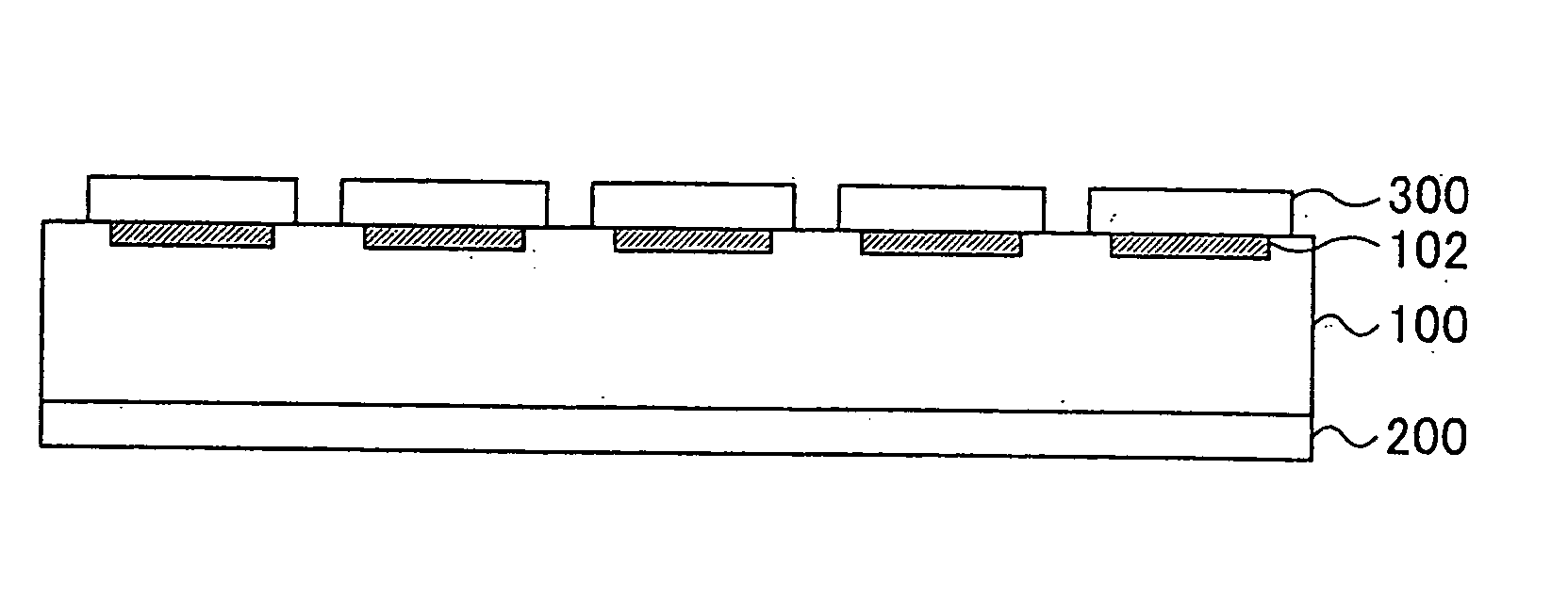
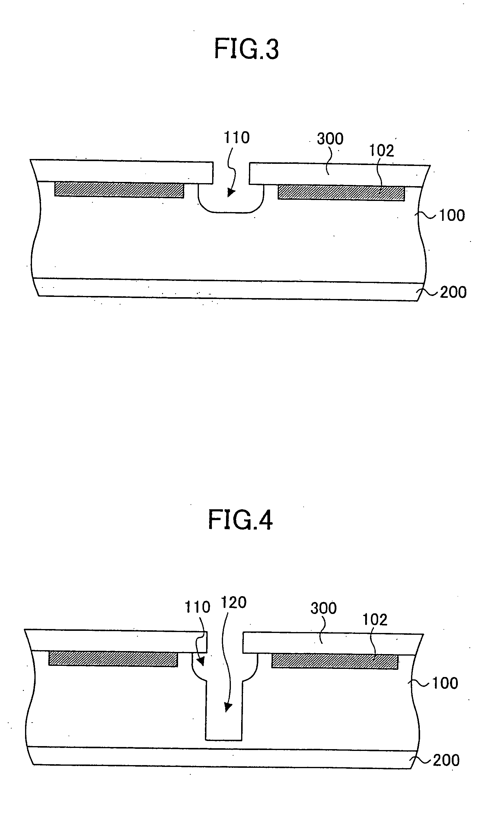
[0030]FIG. 1 shows a first fabrication process of a semiconductor chip according to an embodiment of the present invention. In the first fabrication process, a semiconductor chip fabrication apparatus fixes a semiconductor wafer 100, which is made of silicon and includes two surfaces: an element formation surface (upper side in FIG. 1) having a plurality of semiconductor elements 102 thereon and an element non-formation surface (lower side in FIG. 1) opposite to the element formation surface, by attaching the element non-formation surface of the semiconductor wafer 100 to a tape 200 as illustrated in FIG. 1.
[0031] In addition, the semiconductor chip fabrication apparatus provides a resist film on the element formation surface. Then, by exposing the resist film to light, the semiconductor chip fabrication apparatus removes the portion of the resist film on a c...
PUM
 Abstract
Description
Claims
Application Information