Method and apparatus for bonding a wire

a wire and wire bonding technology, applied in electrical equipment, semiconductor devices, semiconductor/solid-state device details, etc., can solve the problems of unfavorable wire bonding, wire may be swept, and the diameter of the wire used for wire bonding is increased, so as to achieve the effect of increasing the diameter of the wire required

Inactive Publication Date: 2005-09-15
SAMSUNG ELECTRONICS CO LTD
View PDF4 Cites 25 Cited by
  • Summary
  • Abstract
  • Description
  • Claims
  • Application Information

AI Technical Summary

Benefits of technology

[0043] Exemplary embodiments of the present invention provide a method and apparatus for increasing the diameter of a wire required for wire bonding without being limited by the size of a conductive pad for a semiconductor chip.

Problems solved by technology

For example, one problem associated with an MCP may be the diameters of wires used for wire bonding.
In this case, the longer wire may undesirably bend which may come into contact with an adjacent wire of another chip.
Further, another problem associated with an MCP may be that a wire may be swept (e.g., wire being out of position or even losing contact to the chip pads due to the flow of epoxy molding compound (EMC) caused by an injection of the EMC during the molding process of the packaging processes).
However, if the bonding wire 11 becomes longer, then wire 11 may be undesirably bent or swept.

Method used


Image

  • Method and apparatus for bonding a wire
  • Method and apparatus for bonding a wire
  • Method and apparatus for bonding a wire

Examples


Embodiment Construction

[0051] Exemplary embodiments of the present invention will now be described more fully with reference to the accompanying drawings, in which exemplary embodiments of the invention are shown.

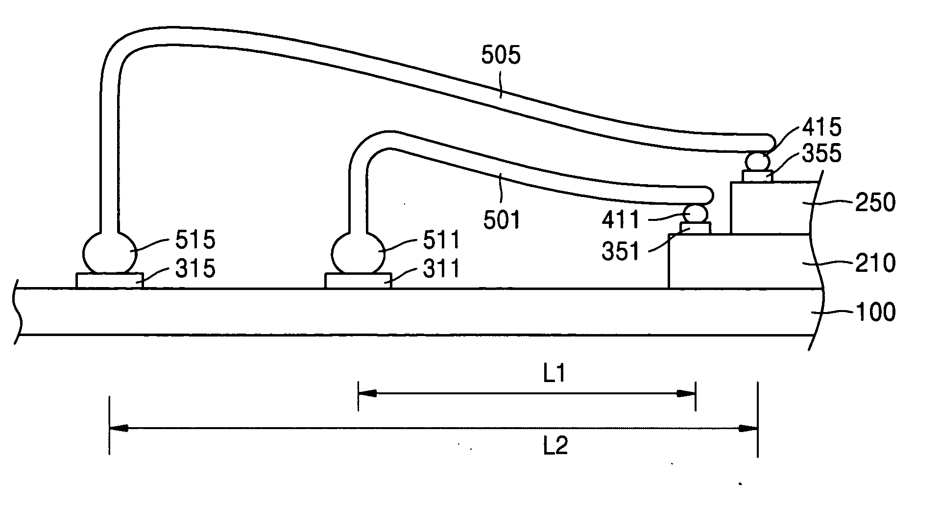
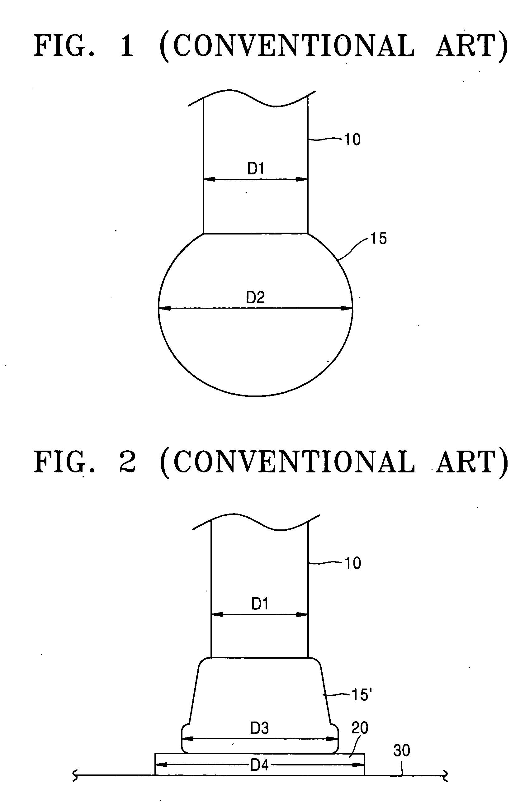
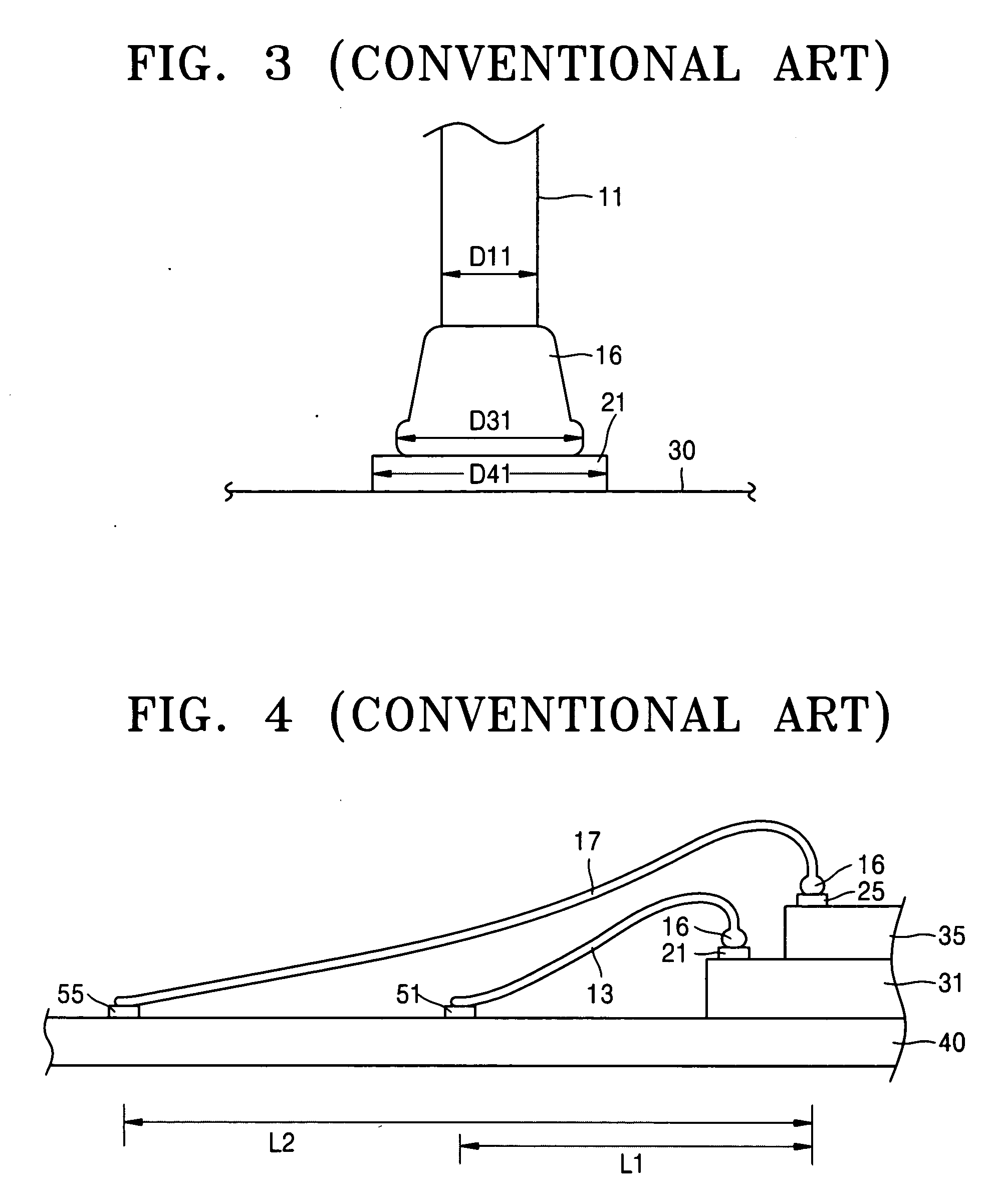
[0052] In at least one exemplary embodiment of the present invention, a small pitch bump may be formed on a pad of a semiconductor chip, and a wire is reversely bonded to the fine pitch bump by a stitch bonding method. With the high integration of semiconductor devices and downscaling of design rules, a wire of sufficient diameter can be used for wire bonding without being limited by the size of the chip pad, even if the size of the chip pad is fine. As a result, when a wire with a small diameter is used, the wire will not bend or be prone to sweeping.

[0053]FIGS. 5 and 6 illustrate a method of bonding a wire on a fine pitch bump using reverse bonding according to at least one exemplary embodiment of the present invention.

[0054] Referring to FIGS. 5 and 6, a reverse wire bonding method may be p...


PUM


Abstract

A method and apparatus for bonding a wire and a wire bond device formed by the same are disclosed. The method includes providing a carrier with at least a first pad, providing a semiconductor chip having at least the second pad, the at least second pad being smaller than the first a pad, forming a conductive stud bump on the second pad, and forming a bonding wire that has two terminal portions, which are respectively bonded to the first pad and the stud bump to electrically connect the first pad and the second pad. The stud bump is bonded to the second pad by a ball bonding method which uses a wire that has an approximately smaller diameter than the bonding wire. Further, a prominence formed on one end of the terminal portions is provided which has an approximately larger diameter than the stud bump.

Description

[0001] This U.S. non-provisional application claims priority under 35 U.S.C. § 119 to Korean Patent Application No. 2004-16414, filed on Mar. 11, 2004, in the Korean Intellectual Property Office, the contents of which are incorporated by reference herein in their entirety.BACKGROUND OF THE INVENTION [0002] 1. Field of the Invention [0003] The present invention relates generally to wire bonding of semiconductor devices, and more particularly, to a method of bonding a wire and a wire bond structure formed by the same. [0004] 2. Description of the Related Art [0005] In recent years, as portable electronic devices have been scaled down (e.g., smaller, thinner and lightweight) where semiconductor devices are used. As such, the process for packaging semiconductor devices has also been scaled down. In these semiconductor devices, a conventional packaging process may include only one semiconductor chip, a multi-chip package (MCP) in which a plurality of semiconductor devices are arranged or...

Claims


Application Information

Patent Timeline
Patent Type & Authority Applications(United States)
IPC IPC(8): H01L21/60H01L23/48
CPCH01L24/03H01L24/05H01L24/45H01L24/48H01L24/49H01L24/78H01L24/85H01L25/0657H01L2224/03H01L2224/04042H01L2224/05599H01L2224/1134H01L2224/32145H01L2224/45015H01L2224/45144H01L2224/48011H01L2224/48091H01L2224/48227H01L2224/48465H01L2224/48471H01L2224/48479H01L2224/48599H01L2224/4903H01L2224/49051H01L2224/78301H01L2224/85051H01L2224/8518H01L2224/85186H01L2224/85986H01L2225/0651H01L2924/01006H01L2924/01079H01L2924/01082H01L2924/19107H01L2924/20752H01L2924/20753H01L2924/00013H01L2924/01033H01L2924/00014H01L2224/48451H01L2224/0401H01L2924/20651H01L2224/13099H01L2924/00H01L2924/181H01L2924/00015H01L2224/4554H01L2224/85399H01L21/60
Inventor KANG, IN-KUAN, SANG-HOYANG, SUN-MO
Owner SAMSUNG ELECTRONICS CO LTD
Why Eureka
Try Eureka