Electron amplifier utilizing carbon nanotubes and method of manufacturing the same

a carbon nanotube and amplifier technology, applied in the manufacture of electric discharge tubes/lamps, electron multiplier details, instruments, etc., can solve the problems of difficulty in conventional electron amplifiers to obtain the desired electron emission efficiency, and achieve the effect of simple manufacturing, high secondary electron emission efficiency

Inactive Publication Date: 2005-09-15
SAMSUNG ELECTRONICS CO LTD
View PDF7 Cites 23 Cited by
  • Summary
  • Abstract
  • Description
  • Claims
  • Application Information

AI Technical Summary

Benefits of technology

[0012] The present invention provides an electron amplifier with an excellent secondary electron emission property, and a method of simply manufacturing an electron amplifier, by which large display device screens can be easily manufactured.
[0018] In the electron amplifier according to the present invention, a secondary electron emission film is formed by mixing carbon nanotubes with a material having a high secondary electron emission efficiency. Thus, the electron amplifier provides a high secondary electron emission efficiency. Also, because the electron amplifier is simply manufactured using a sol-gel method, large display device screens can be economically mass-produced.

Problems solved by technology

Accordingly, it is difficult for conventional electron amplifiers to obtain a desired electron emission efficiency, for example, an electron emission efficiency of 103 through 105 times as much as a primary electron emission efficiency.

Method used


Image

  • Electron amplifier utilizing carbon nanotubes and method of manufacturing the same
  • Electron amplifier utilizing carbon nanotubes and method of manufacturing the same
  • Electron amplifier utilizing carbon nanotubes and method of manufacturing the same

Examples


Embodiment Construction

[0029] The present invention will now be described more fully with reference to the accompanying drawings, in which preferred embodiments of the invention are shown. Throughout the drawings, the same reference numerals denote the same members.

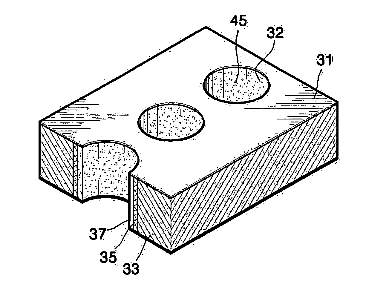
[0030] Referring to FIG. 2, an electron amplifier according to an embodiment of the present invention includes a substrate 33, a plurality of through holes 32 formed in the substrate 33, a resistive layer 35 formed along the inner wall of each of the through holes 32, an electron emission layer 37 deposited on the resistive layer 35 and including carbon nanotubes 45, and upper and lower electrode layers 31 formed on the upper and lower sides of the substrate 33, respectively, so as to be perpendicular to the through holes 32.

[0031] The substrate 33 is formed of glass, ceramic such as Al2O3, or metal such as Cu or Si.

[0032] The resistive layer 35 is formed of metal oxide with sufficient resistance to prevent an electrical short-circuit of the...


PUM


Abstract

An electron amplifier and a method of manufacturing the same are provided. The electron amplifier includes a substrate in which a plurality of through holes are formed, a resistive layer deposited on the sidewalls of the through holes, an electron emissive layer including carbon nanotubes which is deposited on the resistive layer, and an electrode layer formed on each of the upper and lower sides of the substrate. Because the electron emissive layer of the electron amplifier is uniform and provides a high electron emission efficiency, the electron amplification efficiency is improved. The electron amplifier manufacturing method enables economical mass production of electron amplifiers.

Description

BACKGROUND OF THE INVENTION [0001] This application claims priority from Korean Patent Application No. 2002-9088, filed on Feb. 20, 2002, in the Korean Intellectual Property Office, the disclosure of which is incorporated herein in its entirety by reference. [0002] 1. Field of the Invention [0003] The present invention relates to an electron amplifier and a method of manufacturing the same, and more particularly, to an electron amplifier utilizing carbon nanotubes and a method of manufacturing the electron amplifier. [0004] 2. Description of the Related Art [0005] Electron amplifiers include a secondary electron emission layer in order to induce emission of secondary electrons. Electron amplifiers are based on the principle that if primary electrons are accelerated to collide with the secondary electron emission layer, bound electrons on the surface of the secondary electron emission layer absorb the kinetic energy of the primary electrons, and are then emitted as secondary electron...

Claims


Application Information

Patent Timeline
Patent Type & Authority Applications(United States)
IPC IPC(8): H01J9/12H01J1/32H01J43/04H01J43/24
CPCB82Y10/00H01J43/243Y10S977/939H01J2201/30469Y10S977/932H01J43/246C01B32/05H01J43/04
Inventor HEO, JUNG-NAYI, WHI-KUNLEE, JEONG-HEEYU, SE-GIJEONG, TAE-WONLEE, CHANG-SOO
Owner SAMSUNG ELECTRONICS CO LTD
Why Eureka
Try Eureka