Method for fabricating a semiconductor memory cell

a nonvolatile semiconductor and memory cell technology, applied in semiconductor devices, digital storage, instruments, etc., can solve the problems of not being able to integrate a nonvolatile semiconductor memory cell, and achieve the effect of simple and reliable design

Inactive Publication Date: 2005-09-15
ADESTO TECH
View PDF3 Cites 27 Cited by
  • Summary
  • Abstract
  • Description
  • Claims
  • Application Information

AI Technical Summary

Benefits of technology

[0008] Consequently, a central concept of the present invention is to provide the gate electrode device, or gate electrode, or a floating gate electrode required for the selection transistor, namely for the field effect transistor, and the first or bottom electrode device for the memory element as a common material region, either as a whole or in part, thereby producing, without further additional measures, a particular spatial proximity and vicinity of the selection transistor with respect to the actual memory element that is to be addressed by the selection transistor. This also results in a particularly simple fabrication, because the same material region or a part thereof can fulfill two functions, namely, the function of the gate or the gate electrode of the selection transistor, and the function of the bottom electrode for the memory element.
[0023] Consequently, a central concept of the present fabrication method according to the invention is to materially identify the first or bottom electrode device of the semiconductor memory cell or the gate electrode device, and in particular the floating gate electrode of the selection transistor or field effect transistor of the semiconductor memory cell, at least in part or completely with one another in order thereby to achieve a particularly high spatial integration in conjunction with a simplified fabrication method.
[0034] Furthermore, it is advantageous if a spacer layer or corresponding spacer elements covering the wall region of the cutout are formed after the formation of the cutout and prior to the filling of the cutout.
[0041] The method described, constitutes an innovative concept for the integration of a solid electrolyte memory cell and at the same time utilizes a new method for switching and reading from the cell. The method avoids the disadvantages of the active-in-via principle with resistive read-out.
[0042] The combination of a MOS transistor with a solid electrolyte cell in the gate stack achieves a higher tolerance with regard to fluctuations of the resistance value and a faster read-out. Furthermore, a significant improvement in endurance is expected since even metallic bridges formed in weak fashion are sufficient for the ON state. At the same time, the method produces a gain cell with a very small area (4F2) which utilizes all the advantages of a 1T1R cell with respect to a crosspoint architecture without the higher area requirement that is otherwise customary.

Problems solved by technology

It has not previously been possible to integrate a nonvolatile semiconductor memory cell having a storage mechanism based on a solid electrolyte and its fabrication method into a customary semiconductor technology or into a corresponding fabrication method for customary semiconductor technologies without problems.

Method used


Image

  • Method for fabricating a semiconductor memory cell
  • Method for fabricating a semiconductor memory cell
  • Method for fabricating a semiconductor memory cell

Examples


Embodiment Construction

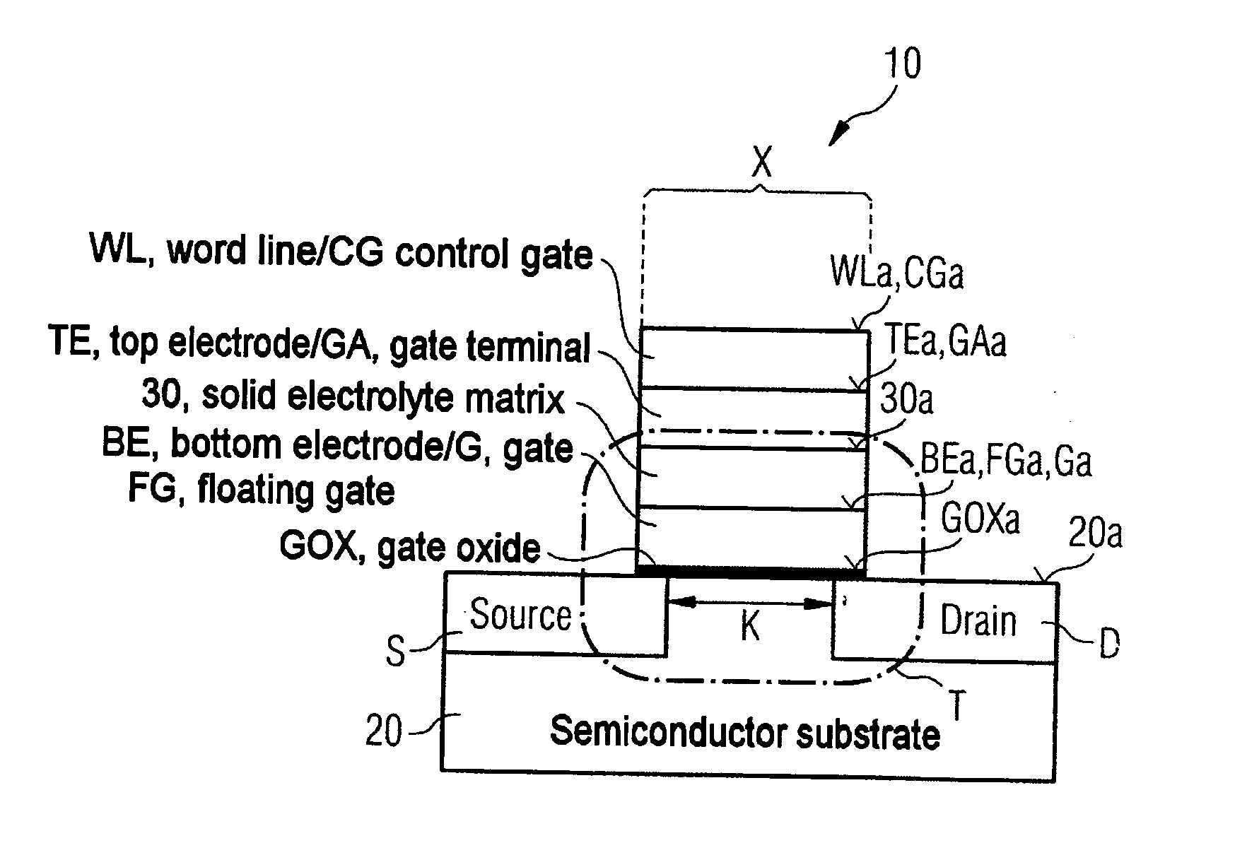
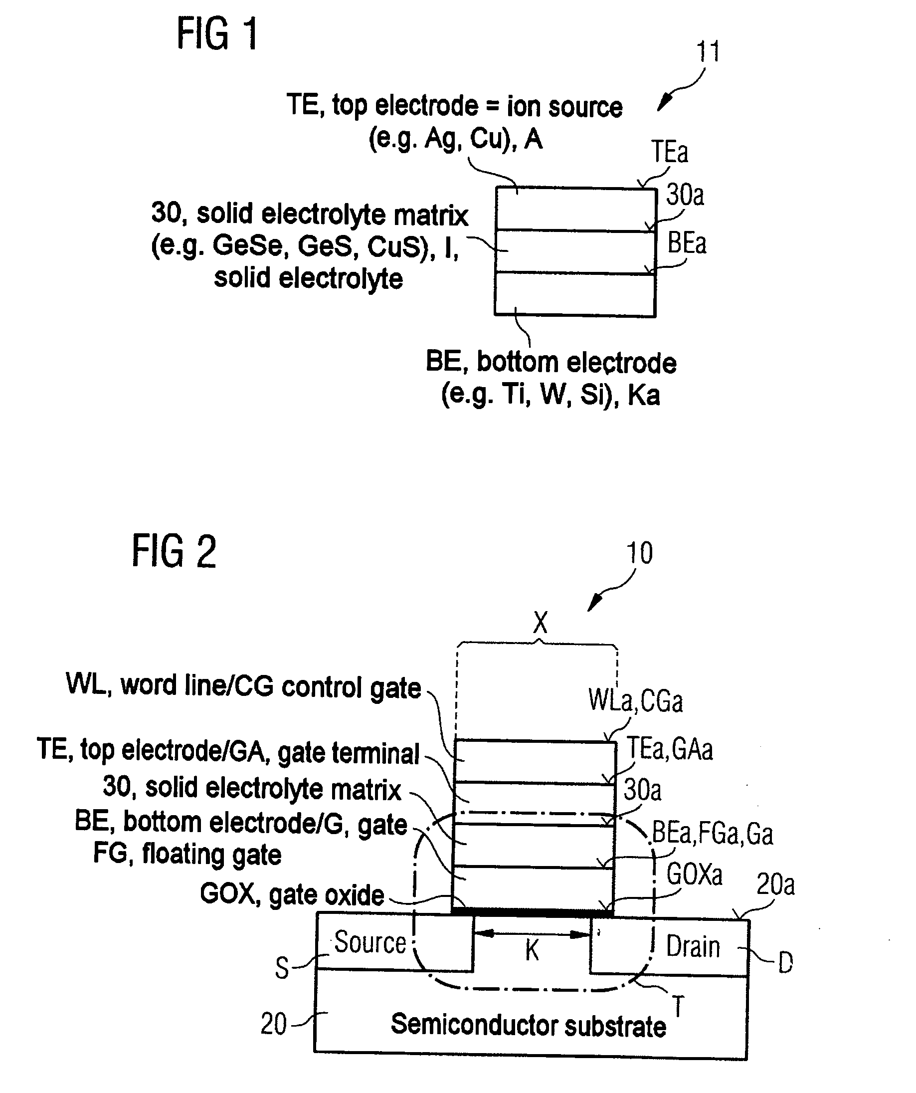
[0054]FIG. 1 shows, in schematic and sectional side view, a memory element 11 of an embodiment of the nonvolatile semiconductor memory cell 10 according to the invention. The memory element 11 illustrated in FIG. 1 comprises a first or bottom electrode BE with a surface region BEa, a solid electrolyte region 30 arranged thereon with a surface region 30a and also a second or top electrode device TE provided thereon with a surface region TEa, which simultaneously serves as ion source or ion reservoir for the solid electrolyte region 30. In the case of the embodiment of the memory element 11 illustrated in FIG. 1, the bottom electrode BE comprises, e.g., titanium, tungsten and / or silicon. The solid electrolyte matrix of the solid electrolyte region 30 comprises GeSe, GeS and / or CuS. The top electrode TE as ion source or as ion reservoir comprises or contains, e.g., Ag and / or Cu.

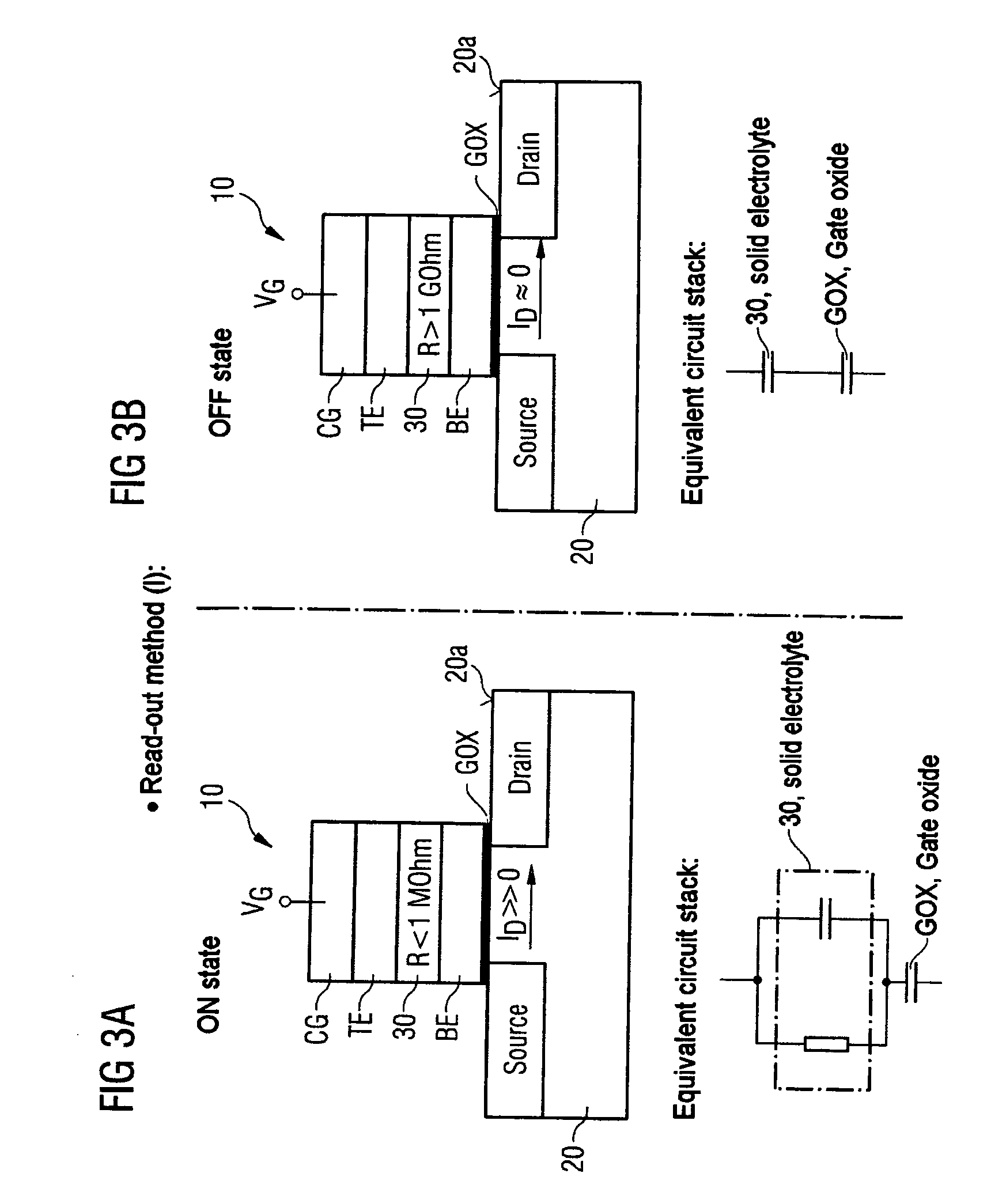
[0055] The memory element 11 illustrated in FIG. 1 can realize two memory states. In state 1, only little me...


PUM


Abstract

Semiconductor memory cell and also a corresponding fabrication method are described, in which a first or bottom electrode device of the memory element of the semiconductor memory cell according to the invention and the gate electrode device of the underlying field effect transistor as selection transistor of the semiconductor memory cell are formed as the same material region or with a common material region.

Description

CROSS REFERENCE TO RELATED APPLICATIONS [0001] This application claims priority under 35 USC §119 to German Application No. DE 10 2004 011 431.5, filed on Mar. 9, 2004, and titled “Method for Fabricating a Semiconductor Memory Cell,” the entire contents of which are hereby incorporated by reference. FIELD OF THE INVENTION [0002] The present invention relates to a method for fabricating a nonvolatile semiconductor memory cell. BACKGROUND OF THE INVENTION [0003] Recent developments in modern semiconductor memory cells include so-called solid electrolyte memory cells, for example, nonvolatile semiconductor memory cells with a storage mechanism based on a solid electrolyte. In these and corresponding fabrication methods, the solid electrolyte region of a memory element can be formed between a first or bottom electrode device and a second or top electrode device. A field effect transistor (FET) can be formed as a selection transistor for addressing the memory element. The FET has a sourc...

Claims


Application Information

Patent Timeline
Patent Type & Authority Applications(United States)
IPC IPC(8): G11C11/24H01L21/8239H01L27/105H01L27/24
CPCH01L27/2436H01L45/085H01L45/143H01L45/1266H01L45/142H01L45/1233H10B63/30H10N70/245H10N70/8416H10N70/8822H10N70/8825H10N70/826
Inventor PINNOW, CAY-UWESYMANCZYK, RALF
Owner ADESTO TECH
Why Eureka
Try Eureka